4F² DRAM becomes server DDR5 RDIMM by year-end
The race to shrink the physical footprint of memory chips is heating up, driven by a groundbreaking shift in semiconductor architecture. At the heart of this revolution is the concept of the 4F² cell, a densely packed design that promises to redefine how data is stored and accessed in memory systems.
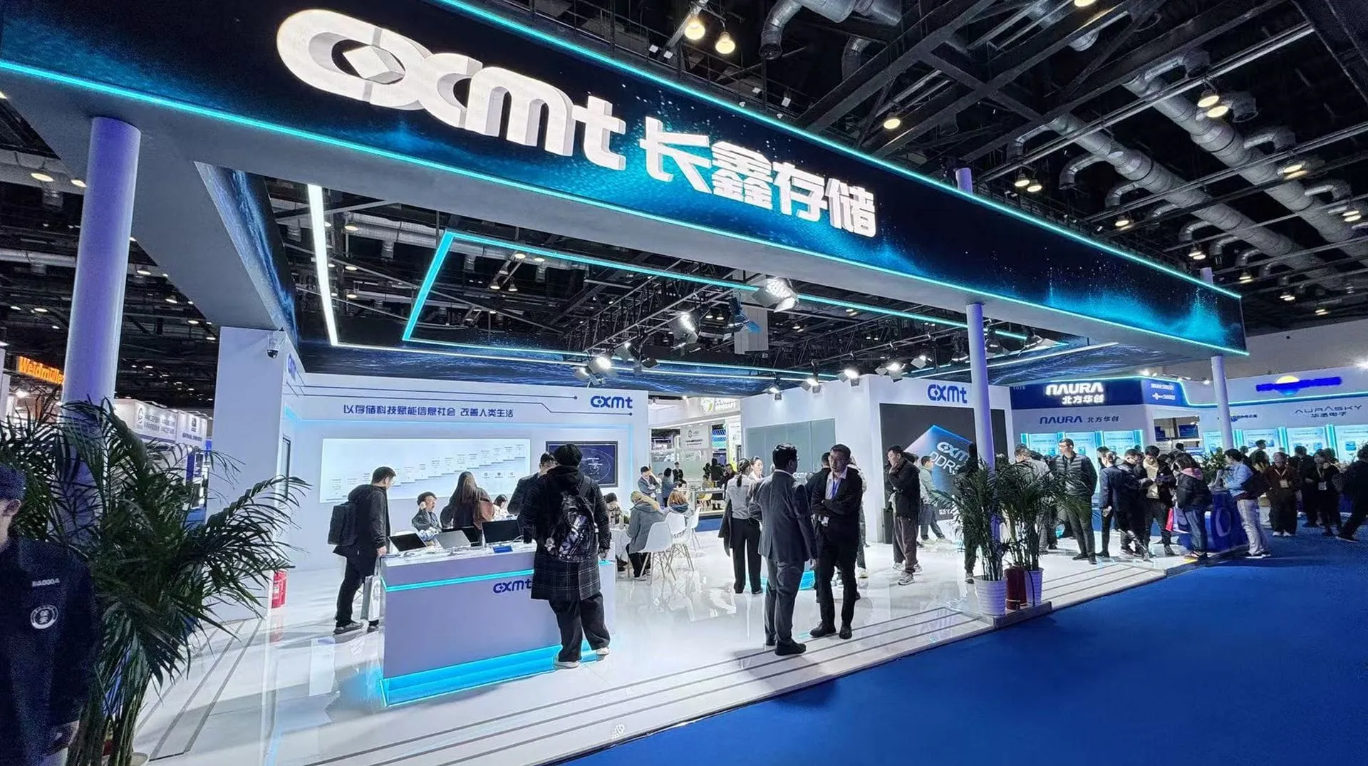
CXMT, a key player in the memory sector, is positioned right at the cutting edge of this evolution. Company president Cao Kanyu recently unveiled plans to launch its first 4F² product—a server DDR5 RDIMM—by the end of the year. This isn’t just an incremental upgrade; it represents a fundamental change in design, built on a denser cell layout that utilizes vertical transistors to dramatically reduce the cell’s footprint by approximately one-third on paper.
The secret to this density lies in ingenious engineering. A 4F² cell is defined as being 2F by 2F, occupying roughly two-thirds the area of traditional 6F² cells at the same feature size. This breakthrough is made possible by novel transistor designs, such as the Vertical Surrounded Gate (VSG) transistor, which features a channel that stands vertically with the gate wrapped around it. This structure allows for much stronger gate control while simultaneously reducing leakage, making the technology significantly more efficient.
CXMT’s intellectual property in this domain is robust, boasting more than 300 published patent families tied to the 4F² technology. This work is part of a broader industry trend where manufacturers are integrating 3D solutions, such as wafer-level hybrid bonding, to decouple the logic and cell density processes. This approach allows for independent optimization of both logic and memory components, pushing the limits of what is possible in semiconductor fabrication.
The competition is fierce, with industry giants also pursuing similar innovations. Samsung, for instance, showcased a 16Gb, 10nm-class 4F² DRAM design using vertical-channel transistors and wafer-to-wafer hybrid copper bonding, aiming for mass production in 2028. Meanwhile, SK hynix is also planning a 4F² vertical-gate platform for its 3D DRAM at advanced nodes.
While the potential of the 4F² architecture is immense, the focus remains firmly on execution. The announcement provides an exciting roadmap, but the full picture—including finalized speeds, capacities, die density, and tested performance metrics—is still forthcoming. Furthermore, scaling this technology from research and patent filings to stable, high-volume production is the next great challenge. With the year drawing to a close, the industry will be keenly watching to see what CXMT delivers in terms of tangible product realization.
Buy on Amazon
Credit
