China builds chips without EUV and the bill keeps growing
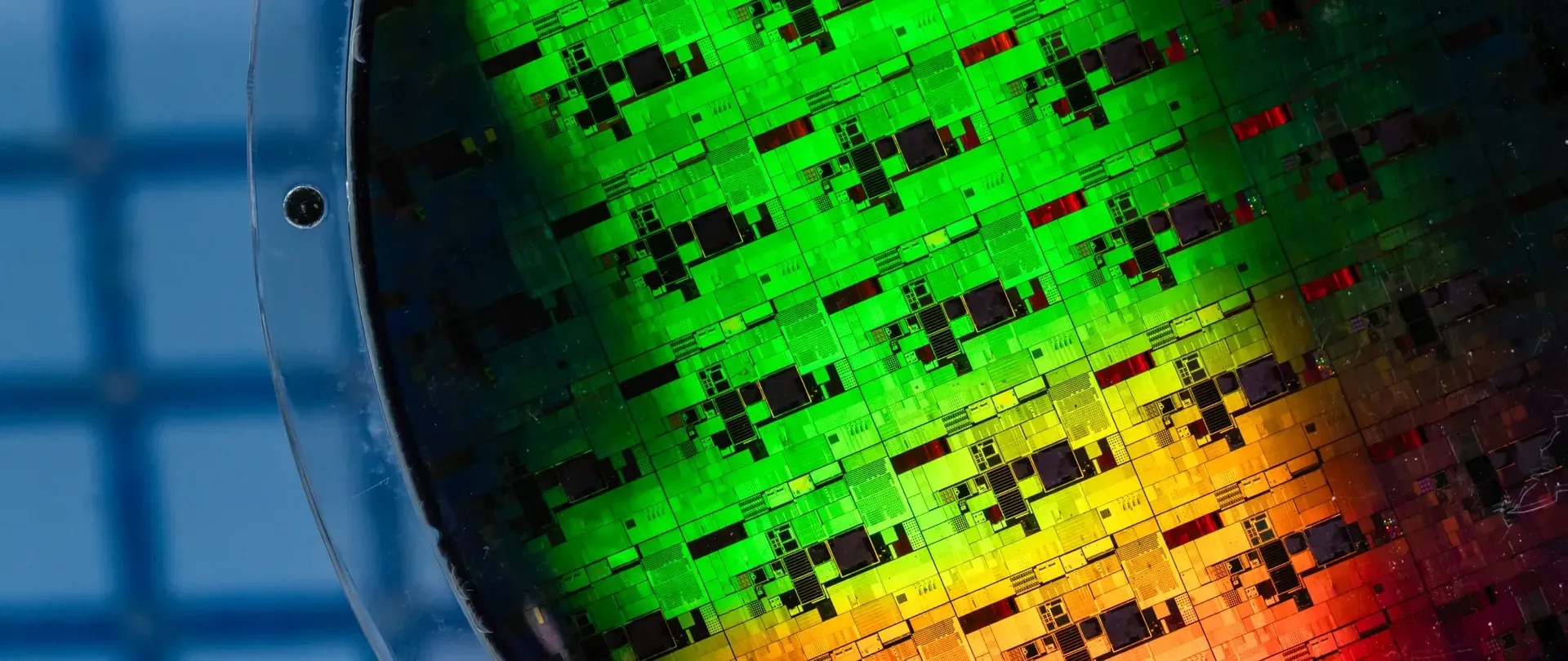
The global semiconductor race is currently defined by a tight geopolitical standoff, specifically over access to the most advanced manufacturing technology: Extreme Ultraviolet (EUV) lithography. Because of stringent export controls, China has been locked out of the cutting-edge EUV machines produced exclusively by Dutch firm ASML, forcing its ambitious chipmaking industry to pivot. Instead of waiting for access, China has channeled its efforts into maximizing the potential of older Deep Ultraviolet (DUV) systems, navigating a complex landscape of engineering compromises.
DUV systems, while not possessing the ultimate resolution of EUV, are surprisingly capable. By employing sophisticated techniques like multiple patterning—dividing complex designs into several simpler layers that are subsequently etched repeatedly—manufacturers can approximate the intricate features required for modern processors. This process is a clever workaround, allowing chipmakers to push the boundaries of what is possible with existing tools.
However, this ingenious workaround comes with significant trade-offs. As lithography expert Chris Mack points out, the shift from a single EUV exposure to multiple DUV exposures introduces complexities. While the theoretical cost calculation might suggest that multiple exposures are manageable, each added step increases the probability of defects and requires tighter process control.
“When this transition began, conventional wisdom suggested that the cost parity between three exposures on a 193 immersion tool and a single EUV exposure was roughly equal,” Mack explains. “But as the complexity grows—as you move from four masks to more—the economic advantage of EUV becomes clearer, and the quality of the final product is directly tied to the ability to manage these accumulating process variations.”
The central challenge lies in efficiency. The ability to create high-performing chips is not just about having the equipment; it’s about yield—how many functional chips can be produced from a wafer. While China has made significant strides in recreating advanced process nodes, such as SMIC’s DUV-based processes, the actual physical scaling often lags behind Western rivals like TSMC and Samsung. This discrepancy highlights a significant efficiency gap in the transition.
Some analysts argue that without access to EUV, the pursuit of leading-edge logic chips faces a hard ceiling. Experts suggest that while DUV can be stretched, particularly in areas like memory where structures are less complex, achieving the densest logic nodes might require innovations beyond current lithography limits. The concept of a “five-nanometer node” is often used, but expert consensus suggests that these terms require careful contextualization.
The story of memory provides a compelling example of where DUV’s efficacy can be maximized. Companies like Micron have demonstrated that through meticulous design and tight process control, they can develop competitive DRAM chips using DUV multiple patterning, effectively pushing the boundaries of older technology. This capability suggests that if the entire immersion ecosystem were available, the industry could make remarkable progress.
Ultimately, the technological wall is not insurmountable, but it is costly. Chinese chipmakers can continue to advance using DUV, but they must accept that pushing the limits of yield and cost will involve larger dies and longer manufacturing times. The reality is that while DUV allows China to keep pace, the full technological leap offered by EUV remains a powerful differentiator in the high-stakes world of advanced semiconductor manufacturing.
Credit
