GlobalFoundries unveils 7nm-class Fusion node after FinFET shift
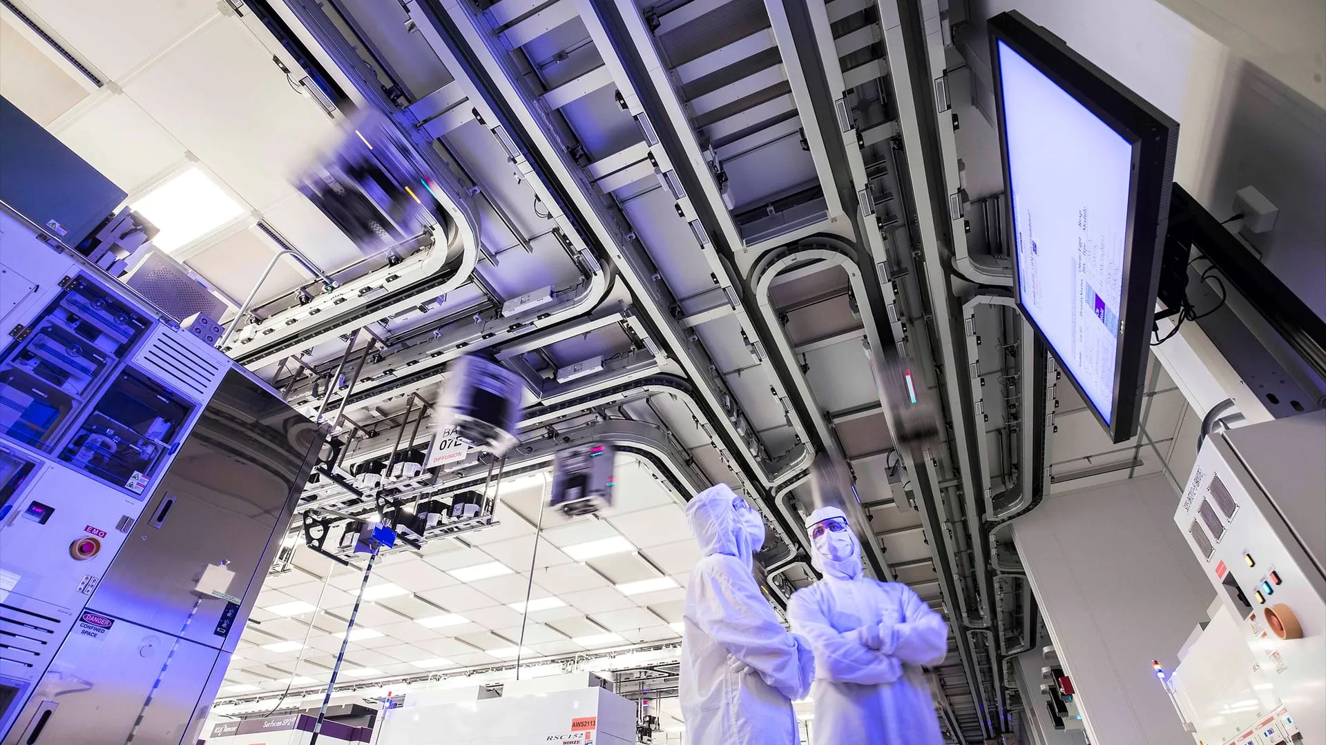
After a brief pause in the pursuit of the most advanced semiconductor nodes, GlobalFoundries is making a bold comeback. Eight years after shelving development on leading-edge nodes, the company is now returning to the forefront of fabrication with a revolutionary approach: the FDX Fusion process.
This new technology doesn’t rely on traditional FinFET structures but instead leverages planar transistors and fully-depleted silicon-on-insulator (FD-SOI) architecture. This shift is specifically aimed at applications that prioritize efficiency, integration, and cost-effectiveness—perfect for demanding sectors like automotive, edge AI, industrial robotics, and advanced sensing devices.
The promise of FDX Fusion is immense. It aims for 7nm-class digital performance and boasts more than twice the transistor density of the previous 22FDX process. But the real genius lies not just in the performance metrics, but in what the technology allows engineers to achieve: combining complex circuitry onto a single chip.
FDX Fusion is designed to seamlessly integrate digital logic with RF, analog, and mixed-signal components, alongside embedded nonvolatile memory and in-memory computing capabilities. This powerful combination is the key to creating highly integrated System-on-Chips (SoCs) that can handle complex sensor data, execute AI inference, and manage wireless communication without needing multiple separate components. Essentially, FDX Fusion aims to drastically reduce system complexity and power consumption.
This level of integration is what GlobalFoundries calls the process technology. By unifying these disparate functions, the technology potentially bypasses the costly and power-hungry process of manufacturing multiple chips on different process nodes, streamlining the entire design and production workflow.
The roadmap for FDX Fusion is ambitious. GlobalFoundries plans to deliver initial demo silicon for customer evaluation in early 2027, followed by the first process design kit (PDK) in mid-2027. The company intends to bring production capabilities to its Dresden, Germany, facility in 2028, marking a significant step in its evolution beyond the 22nm-class platform.
The potential impact extends far beyond the chips themselves. FDX Fusion could offer European semiconductor developers a powerful alternative to reliance on leading-edge foundries in Asia or the United States. It could democratize access to advanced manufacturing techniques for the European ecosystem.
The excitement is already translating into industry interest. Major players in the automotive and industrial sectors, including BMW, Bosch, Infineon, NXP, Siemens, and Tesla have expressed interest in leveraging FDX Fusion. This interest is particularly focused on specialized areas like radar and wireless communications, where the efficiency gains are paramount.
While the technology holds incredible promise, the journey to full commercial success will depend on several factors. The actual performance numbers, density, and production costs will be critical benchmarks. Furthermore, for FDX Fusion to truly reshape the industry, GlobalFoundries must foster a robust ecosystem of Electronic Design Automation (EDA) tools and silicon-proven building blocks to attract the broader range of chip developers looking to utilize this innovative platform.
Buy on Amazon
Credit