Intel’s EMIB and Foveros packaging roadmap analysis
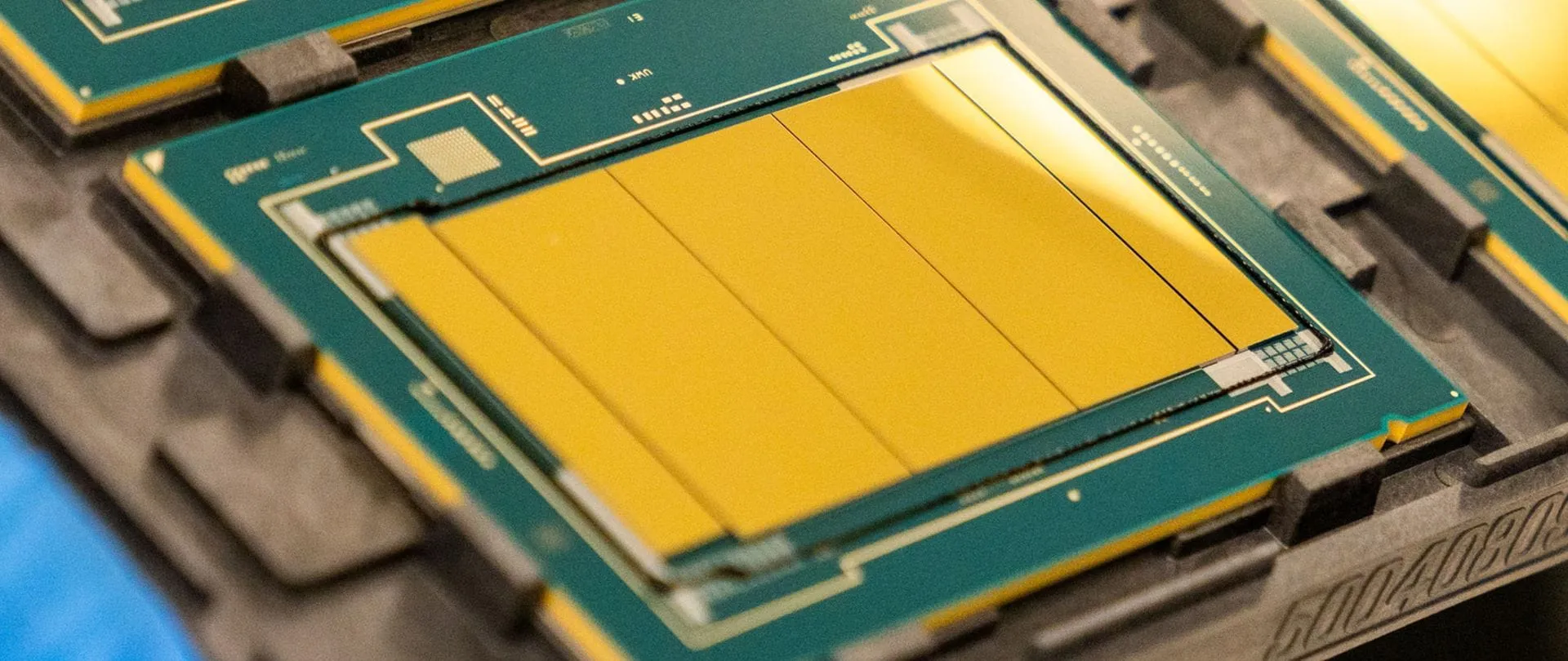
The provided text outlines Intel’s strategy for advanced heterogeneous integration and scaling through its packaging technologies, primarily focusing on the Foveros and EMIB families. The roadmap progresses from traditional microbumps to direct copper bonding, ultimately aiming for massive, tightly coupled 3D System-in-Packages (SiPs).
Here is a synthesis of the key technologies and their implications:
—
1. Foveros: The Foundation for 2.5D and Heterogeneous Integration
The Foveros family focuses on enabling high-density, cost-effective chiplet communication:
Foveros 2.5D: This technology uses 36 µm microbump pitches but is designed to scale down to pitches below 25 µm. It supports high bump density scaling (772 to 1,600/mm²) and extremely low power consumption (0.15 pJ/bit). It is slated for production readiness in 2027.
Foveros-B: This extends the concept for larger AI/HPC designs by combining RDLs with local active or passive silicon bridges. It aims to provide an intermediate option between RDL-only and large silicon interposers, positioning it as a competitor to TSMC’s CoWoS-R.
Performance Metrics: Both Foveros technologies are designed to achieve high density and low power, with Foveros-B and the Direct 3D evolution aiming for pitches below 25 µm and power below 0.15 pJ/bit.
2. Foveros Direct 3D: Eliminating Bumps for Ultimate Density
Foveros Direct 3D represents the architectural shift from traditional microbumps to direct copper-to-copper hybrid bonding, which is essential for next-generation scaling:
Core Concept: It eliminates solder bumps entirely by directly bonding copper pads between dies. This method allows for significantly finer interconnect pitches (below 10 µm) than conventional microbumps, offering up to 10 times finer connections.
Advantages:
Density & Pitch: Supports pitches as fine as 3 µm in the second generation.
Interconnect Quality: Achieves extremely low power consumption (e.g., <0.05 pJ/bit for 1st Gen).
Thermal Management: Direct bonding creates more continuous thermal paths, which is crucial for managing the high power density in stacked logic.
Application: Intel’s Xeon 6+ processor uses this technology, planning to shrink the bonding pitch from 9 µm (1st Gen) down to 3 µm (2nd Gen).
3. EMIB: The Horizontal Interconnect Layer
EMIB (Embedded Multi-die Interconnect Bridge) provides the high-bandwidth horizontal connectivity necessary to link these densely packed modules:
Role: EMIB acts as the high-bandwidth layer connecting the smaller, densely integrated chiplet assemblies (Foveros) horizontally.
Integration (EMIB 3.5D): The ultimate goal is to combine Foveros (for dense vertical connectivity) with EMIB (for horizontal links) to create EMIB 3.5D.
System-in-Package (SiP) Scaling: EMIB 3.5D allows Intel to scale large heterogeneous systems—such as the Ponte Vecchio GPU—by providing massive connectivity without relying on enormous, monolithic silicon interposers.
4. The Ultimate Architecture: EMIB 3.5D
The combination of Foveros and EMIB culminates in the EMIB 3.5D architecture:
Vertical Integration (Foveros): Provides dense, local 2.5D or 3D connectivity within individual chiplet assemblies.
Horizontal Scaling (EMIB): Provides high-bandwidth connections between these assembled modules.
Outcome: This synergy allows Intel to scale complex processors both vertically and horizontally, enabling massive AI and HPC applications in highly integrated systems.
Summary of Scaling Trajectory
Intel’s roadmap is defined by a progression towards denser, more energy-efficient, and more flexible packaging:
1. Start (Foveros 2.5D): Dense chiplet interconnects via microbumps.
2. Mid-Step (Foveros Direct 3D): Transition to direct copper bonding for ultra-fine pitches and superior thermal management.
3. Final Goal (EMIB 3.5D): Combining vertical density (Foveros) with massive horizontal bandwidth (EMIB) to create large, heterogeneous System-in-Packages that scale beyond the limits of traditional silicon interposers.
Buy on Amazon
Credit