Micron cancels future 4F² DRAM after 20 years of research
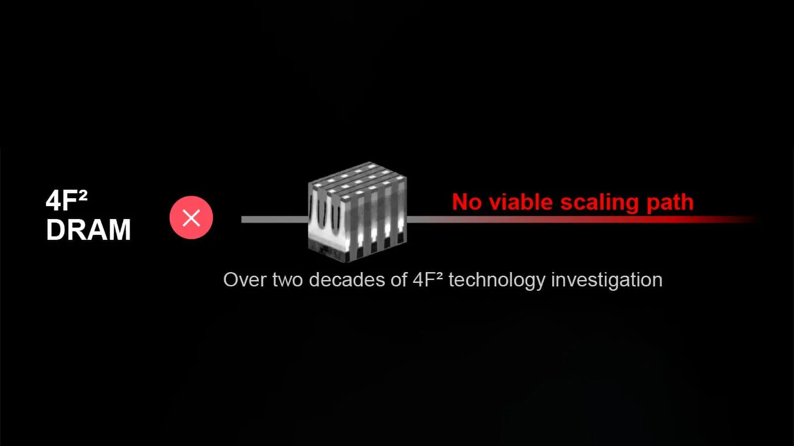
For decades, the quest for 4F² memory cells has been viewed by the DRAM industry as a holy grail. This architecture promised a revolutionary leap in density, aiming to reduce the physical area of a memory cell by 33% compared to conventional 6F² designs, theoretically allowing for a massive increase in the number of memory cells packed onto a single chip.
But as the industry pushed the boundaries of manufacturing, even the most ambitious theoretical paths eventually collided with the realities of physics and engineering. Micron, a pioneer in this space, has reached a pivotal conclusion: the pursuit of 4F² DRAM does not offer the promised density advantages and instead introduces significant manufacturing complexity and cost. Consequently, the company has decided to focus its future scaling strategy elsewhere.
“Micron invented 4F² DRAM,” stated Scott DeBoer, president and chief technology and products officer at Micron. “The path with 4F² DRAM was always an option, but we evaluated it and chose not to pursue it due to the increased complexity and cost over the past two decades.”
The allure of the 4F² concept lies in its simple mathematical appeal. The notation refers to a cell area equivalent to four times the square of the minimum lithographic feature size (F), compared to the six times F² used in standard DRAM. In theory, this meant a potential 50% increase in memory cells per wafer.
However, the true bottleneck lies not in the transistor area itself, but in the surrounding architecture. Experts note that the practical limits of memory density are determined by the capacitor pitch, the size of the capacitor, and overall dimensions, rather than simply the nominal area of the transistors. To achieve real density gains, DRAM makers must manage the arrangement of capacitors, which imposes constraints that often negate the benefits of smaller transistor footprints.
This realization shifts the focus back to the proven architecture. Micron now plans to continue scaling conventional 6F² DRAM, believing that density gains can be achieved by refining the capacitor pitch and shrinking process technologies, rather than introducing a fundamentally new transistor structure. Advanced lithography and materials will continue to drive incremental improvements.
For instance, Micron is actively pursuing next-generation processes like the 1δ process technology, which is slated to enter volume production in the latter half of 2027 and promises a mid-20% improvement in bit density over current standards. Furthermore, the industry is looking toward High-NA EUV lithography for future generations.
Ultimately, the long-term vision for DRAM density may not be found solely in refining planar scaling. Micron’s preferred trajectory is toward 3D DRAM, where memory cells are stacked vertically. While both Samsung and SK hynix maintain 4F² options in their roadmaps, Micron is betting that layering memory vertically will offer the optimal balance of density, cost, and manufacturing complexity needed to define the next era of memory technology.
Buy on Amazon
Credit