Micron doubles bit density with 400+ layer 3D NAND
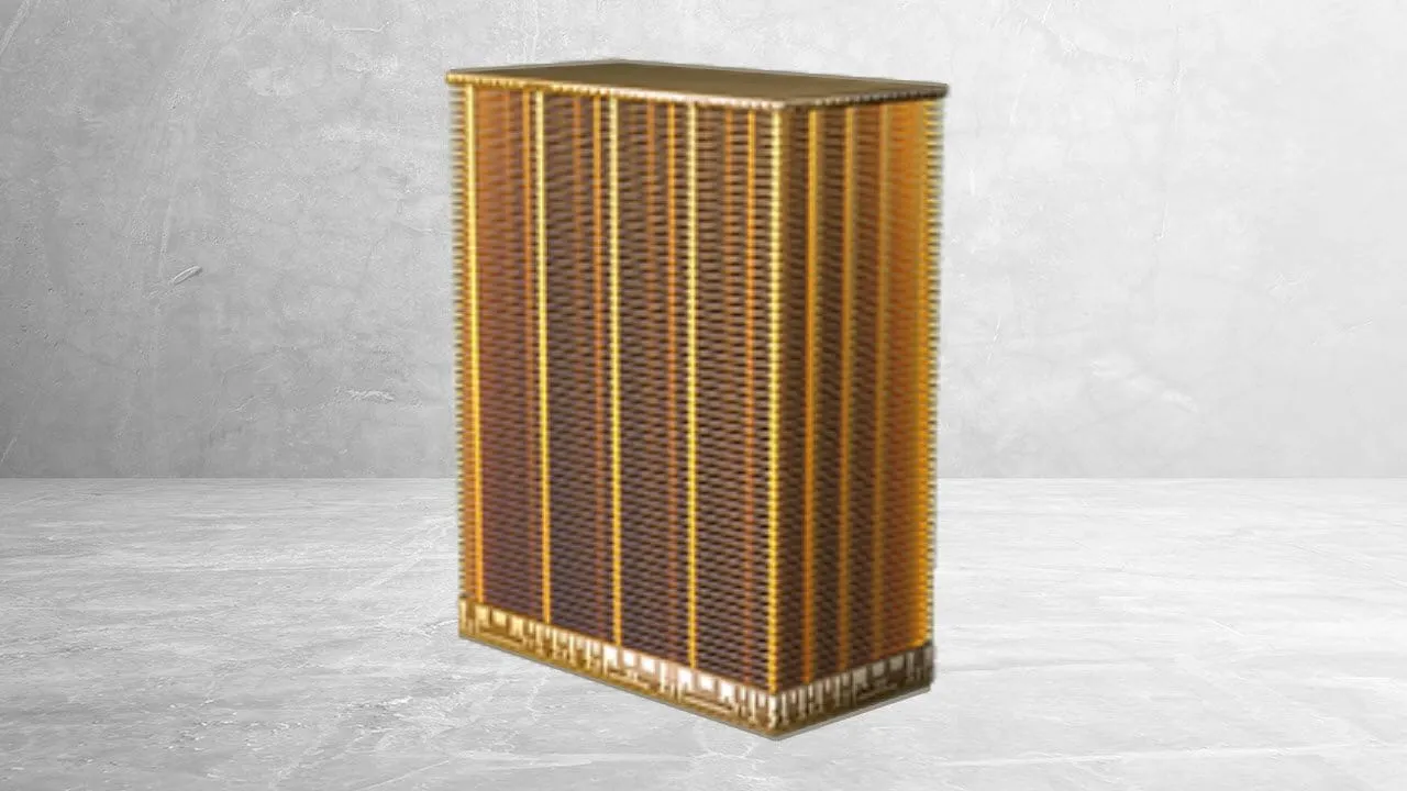
The relentless pursuit of faster, denser, and more efficient memory is taking center stage in the semiconductor world, and Micron is leading the charge. The company has unveiled plans for its next-generation 3D NAND, a leap forward that promises to redefine how we store and access data. Set to enter mass production in the second half of 2027, this technology isn’t just an incremental update; it’s a complete architectural overhaul.
Micron‘s G11 technology is poised to deliver three massive advantages for consumers and data centers. First, it will double storage density, meaning more capacity packed into the same space. Second, I/O performance will see a staggering 50% increase compared to the previous generation. Finally, the process will significantly decrease power consumption, tackling the growing energy demands of modern computing.
To achieve these ambitious goals, Micron is leveraging cutting-edge techniques. Central to this advancement is the adoption of wafer-on-wafer bonding. This innovative method allows the company to construct the NAND array and the logic fabrication process on separate wafers before bonding them together. This flexibility is key, enabling the independent optimization of memory arrays and peripheral circuits, leading directly to superior capacity and performance.
The technical specifications of G11 highlight this breakthrough. It represents the world’s most advanced NAND technology, pushing the boundaries of storage density. For instance, the new generation is projected to achieve approximately twice the bit density of its predecessor, with the density jumping from 3D TLC 21 Gb/mm to 3D TLC 42 Gb/mm. Furthermore, the technology will boost I/O speeds, increasing them from 3,600 MT/s to 5,400 MT/s, while simultaneously reducing the energy consumed per bit by more than 25%.
This kind of performance gain is critical. It means that everything from conventional high-capacity SSDs to emerging AI-oriented storage devices will benefit from drastically improved bandwidth and energy efficiency. The shift is designed to handle the massive data throughput required by today’s demanding applications.
Beyond simply stacking more layers, Micron is also innovating at the fundamental level. The G11 architecture transitions to supporting more than 400 NAND layers, suggesting that density gains will come from a holistic approach—combining increased layers with smaller memory cell dimensions. This focus on density enhancement through architectural refinement is what will keep pace with the industry’s relentless scaling demands.
Looking ahead, the company’s roadmap extends far beyond G11. Micron is heavily invested in developing breakthrough high-mobility materials and denser cell architectures. The future of 3D NAND scaling will increasingly rely on innovations in materials and cell design, rather than simply adding more layers. This focus on XYZ scaling—shrinking the dimensions—is the path forward, promising even greater efficiency and capacity in the years to come.
Credit
