Russian firm makes first 130nm chipmaking tool
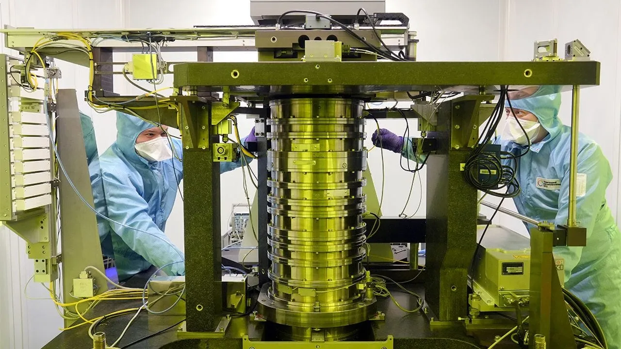
The race for the next generation of microchips is heating up, and in the quest for technological independence, a significant milestone has been achieved in Russia’s semiconductor sector. The Zelenograd Nanotechnology Center (ZNTC) has successfully completed the third research and development stage for its first lithography tool capable of processing 200-mm wafers using a cutting-edge 130nm process technology.
This achievement isn’t just a technical exercise; it represents a major leap in domestic engineering capability. Experts suggest that the development of this system demonstrates that Russia possesses the deep engineering expertise required to design and construct sophisticated lithography equipment, opening the door for future efforts to target even smaller process nodes like 90nm and 65nm.
The development of this ambitious system was a massive collaborative effort. While the ZNTC handled the overall system development, design, process modeling, and equipment development, the Belarus-based Planar played a crucial role in developing the core lithography system itself. This collaboration, supported by approximately 70 million dollars allocated by the Ministry of Industry and Trade, showcases a coordinated push into advanced microelectronics.
The project involved intricate engineering across the board. Planar was responsible for manufacturing the mechanical assemblies and components, while Lassard developed the necessary laser light source. ZNTC was tasked with the complex calculations, projection-lens design, and developing the critical process modeling required for the equipment to function.
From a financial perspective, the scale of the endeavor is considerable. Estimates place the cost of a single 130nm-capable ZNTC stepper, including its specialized laser source, around $7.3 million. When measured against historical benchmarks, this places the investment in a fascinating context, demonstrating an impressive level of engineering at a time when global technology races are intensifying.
While this prototype is a triumph of engineering, the journey from laboratory prototype to mass production line is long. The current machine is still an engineering prototype, undergoing rigorous internal testing to validate imaging, overlay, reliability, and throughput. This critical validation phase is expected to take well over a year.
Experts suggest that even established industry players require several years to transition from an integrated engineering system to full production deployment. Consequently, a realistic timeframe for the Russian machine to begin processing commercial wafers and entering the mass semiconductor market is likely around 2029 at the earliest.
Despite the lengthy road ahead, this project firmly establishes Russia’s position in the high-tech microelectronics landscape. It is a powerful demonstration that sophisticated, advanced lithography capabilities can be developed domestically, laying essential groundwork for future innovation and industrial growth in the field.
Buy on Amazon
Credit