Tower invests $4B to build massive optical connectivity hub in Japan
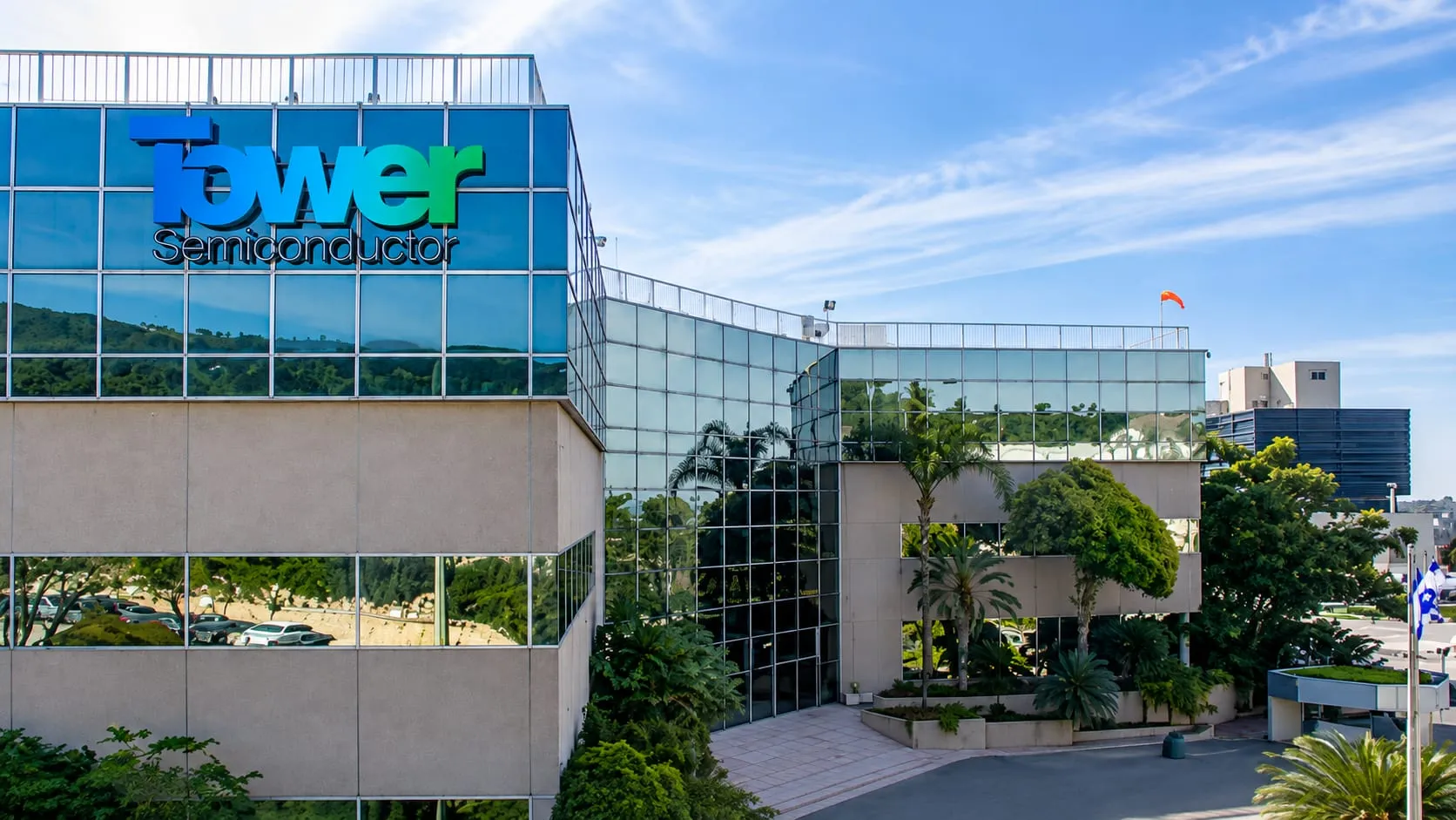
The global race for optical connectivity—the backbone of modern AI infrastructure—is fueling an ambitious industrial pivot in Japan. Tower Semiconductor and the Japanese government are embarking on a monumental $4 billion co-investment designed to transform regional fabrication facilities into a colossal manufacturing hub for optical-connectivity semiconductors.
This strategic expansion is not just about adding capacity; it’s about fundamentally reshaping how advanced photonics are produced. The plan involves repurposing existing facilities and building new ones to create a massive base capable of meeting the surging demand for optical engines used in the burgeoning AI sector.
The vision is dual-tracked. Track One focuses on conversion and immediate expansion. This involves taking Tower’s idle 200-mm Fab 6 in Arai, Niigata Prefecture, and transforming it into a state-of-the-art 300mm manufacturing facility for silicon photonics (SiPho) and complex optical packaging. Simultaneously, they aim to maximize output from the existing 300mm Fab 7 near Uozu, Toyama Prefecture, which is already producing critical components like silicon-germanium electronic integrated circuits (SiGe EICs).
Fab 7 is already a powerhouse, manufacturing advanced nodes using technologies like the latest TPS65SG and TPS45PHD fabrication nodes. The strategy here is to progressively scale production by installing additional equipment, allowing the company to meet growing demand for optical engines without waiting years for entirely new process flows to qualify.
Track One is slated for full production readiness by the fourth quarter of 2027, with projections indicating substantial financial growth, expected to yield approximately $3.6 billion in revenue and $1.2 billion in net profit by fiscal year 2028.
The ambition doesn’t stop there. Track Two is significantly more ambitious: constructing an entirely new 300mm manufacturing facility adjacent to Fab 7. This second stage will dramatically multiply the company’s output of SiGe EICs and SiPho PICs, positioning Tower with two major sites in Japan dedicated to these advanced semiconductor products.
By 2029, this integrated effort is expected to boost Tower’s Japanese production capacity to the equivalent of 45,000 300mm wafers per month—a staggering increase of over 40 times the 2025 levels. This massive scale reflects the reality that Tower commands more than 80% of the contract production market for optical communications semiconductors used in servers, making this expansion a necessity, not a luxury.
The investment, which is shared between Tower’s own $3 billion and Japan’s $1 billion contribution from the Ministry of Economy, Trade and Industry (METI), underscores the strategic importance of the project. Beyond capacity, the initiative is a critical move for setting the stage for future technologies like co-packaged optics (CPO), bringing cutting-edge manufacturing technologies closer to the world of compute silicon.
This massive undertaking is intertwined with a significant restructuring of Tower’s local operations. By taking full operational control of key facilities like Fab 7 and Fab 6, Tower is evolving its relationship with its partners, consolidating the former structure to create a cohesive, industry-leading 300mm SiPho and SiGe production hub in Japan.
Buy on Amazon
Credit