LG’s maskless laser machine speeds up chip packaging
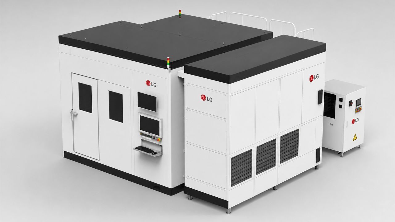
The high-stakes world of semiconductor manufacturing is rapidly evolving, with advanced packaging technologies like EMIB and CoWoS becoming critical battlegrounds. As chip designers seek alternatives to traditional constraints, outsourced semiconductor assembly and test (OSAT) companies are pushing the boundaries of tools, introducing novel methods to deliver superior yields and performance.
Joining this technological fray is LG, which is making a significant push into the domain of advanced patterning with its Laser Direct Imaging (LDI) system. This initiative places the company directly into the competitive landscape of direct-imaging, a field currently dominated by industry giants like KLA, Screen Holdings, and others.
LG has recently solidified this ambition by signing a contract with an OSAT to supply it with an LDI lithography tool. This machine is designed to build intricate metal-interconnect patterns required for sophisticated semiconductor packaging, potentially offering yields that surpass current available tools.
At the core of this innovation is the LDI system itself: a maskless lithography machine that uses a laser to project a digitally generated circuit pattern directly onto a photoresist-coated substrate. Unlike traditional methods that rely on physical photomasks, LDI acts much like a laser cinema projector, beaming a digital image onto the material to define where metal wiring will form.
This technology offers a powerful advantage: it is dynamic. Because the image is generated and calibrated digitally in real time, the system can precisely adjust patterns to account for variations in the substrate—such as organic materials that expand or contract during processing. This ability to compensate for substrate peculiarities is a game-changer, minimizing potential defects like solder bridges and drastically improving yield loss.
With the latest LDI technology, LG’s equipment can achieve line-and-space patterns down to 1.5-µm, setting it at the high end of the current market. While this may not match the ultimate resolution of cutting-edge systems like EUV or e-beam lithography, LDI trades absolute resolution for vastly increased throughput and the ability to process large areas, which is exactly what production demands.
The flexibility of LDI allows it to pattern Redistribution Layers (RDL) interposers used in next-generation technologies like TSMC CoWoS-R/-L, where rivals offer various pitch options. The ability to handle 1.5-µm patterning makes LDI a highly relevant tool for the complex demands of chip packaging.
Crucially, LG is not entering this market from scratch. The company already possesses deep experience, having successfully commercialized LDI technology for display manufacturing. This means the semiconductor packaging-grade equipment represents an exciting expansion of existing LG expertise rather than a pure leap into an unproven field.
Looking ahead, this move is just the beginning. LG plans to expand its portfolio into other high-demand areas, including high-bandwidth memory (HBM) inspection equipment and through-glass-via (TGV) laser systems for glass substrates. While establishing itself against established players will take time, this new player provides much-needed capacity and competition for the semiconductor ecosystem.
Buy on Amazon
Credit
