TYLsemi raises $43M for custom silicon
Unpacking the AI Silicon Revolution: How a Startup is Rewriting the Rules of Custom Chips
The race for cutting-edge artificial intelligence hardware demands ever-more complex and specialized custom processors, yet the traditional method of designing monolithic silicon faces staggering challenges in terms of cost, time, and yield. Enter TYLsemi, a new semiconductor firm that is aggressively tackling this complexity by championing a modular approach to AI infrastructure development.
With $43 million in early-stage funding, TYLsemi is not just another custom ASIC design house; they are building an ecosystem designed to simplify the path for companies seeking to build multi-chiplet systems. Their ambition is to provide reusable, standards-based connectivity and power delivery that allows developers to focus on their unique compute logic rather than wrestling with intricate physical implementations.
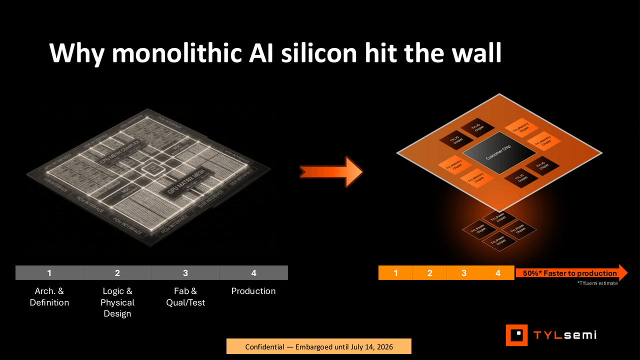
The shift is driven by fundamental changes in semiconductor manufacturing. As chip sizes grow toward the limits of modern process nodes, achieving high yields becomes exponentially more difficult. TYLsemi argues that combining smaller, specialized components—or chiplets—with advanced packaging techniques offers a viable and economically superior alternative to monolithic designs.
At the heart of their innovation is the belief that modularity is the future for AI accelerators. Companies building massive AI infrastructure need flexibility and resilience. TYLsemi addresses this by offering an end-to-end service, enabling even teams without deep silicon expertise to design, implement, package, qualify, and mass-produce their own multi-chiplet processors.
Co-founded by semiconductor veterans who have led engineering and business teams at industry giants like Cadence and Rambus, TYLsemi brings unparalleled experience with both standard and custom silicon. Their founders contend that the time is now to embrace chiplets, leveraging advancements in die-to-die standards like UCIe to create a practical path forward.
To make this vision tangible, TYLsemi has developed a suite of foundation chiplets designed as reusable building blocks. These include TYL.IO for high-speed connectivity (like PCIe and CXL), TYL.Power for integrated power delivery solutions, and the planned TYL.Mem family for memory integration. These components are built using various process technologies from foundries like TSMC.
The true magic lies in their TYL.Forge platform. This system allows customers to bring their proprietary compute architecture—such as matrix-multiplication engines—to TYLsemi, who then handle the complex physical implementation and integration with the standardized chiplets. This dramatically reduces risk and accelerates time to market by eliminating the need for customers to reinvent common functions like I/O or power delivery.
This approach delivers significant economic advantages. TYLsemi estimates that their multi-chiplet strategy can reduce the total cost of ownership by up to 57% when scaling to high volumes, turning a complex monolithic design into an integrated System-in-Package (SiP). By reusing pre-validated silicon and lowering per-unit costs, they aim to slash development cycles—potentially shrinking multi-year custom silicon programs into six to nine months from a mature design to tape-out.
TYLsemi’s focus is firmly on AI infrastructure, targeting data-center CPUs, high-performance computing, and networking. While acknowledging that chiplets are already being used in consumer GPUs, they see the vast potential for heterogeneous integration within the rapidly expanding world of AI accelerators. By prioritizing standardized interfaces and reusable components, TYLsemi is positioning itself to provide the scalable, resilient silicon foundations necessary for the next generation of AI-era processors.
Credit
