ASML ditches particle tech for laser plasma chipmaking
The future of microchips hinges on light. Specifically, the development of Extreme Ultraviolet (EUV) lithography scanners requires an almost impossible feat of physics and engineering: creating a powerful, stable, and reliable light source. For the industry, this challenge boils down to a fierce technological rivalry between two distinct approaches to generating the necessary 13.5-nm EUV radiation.
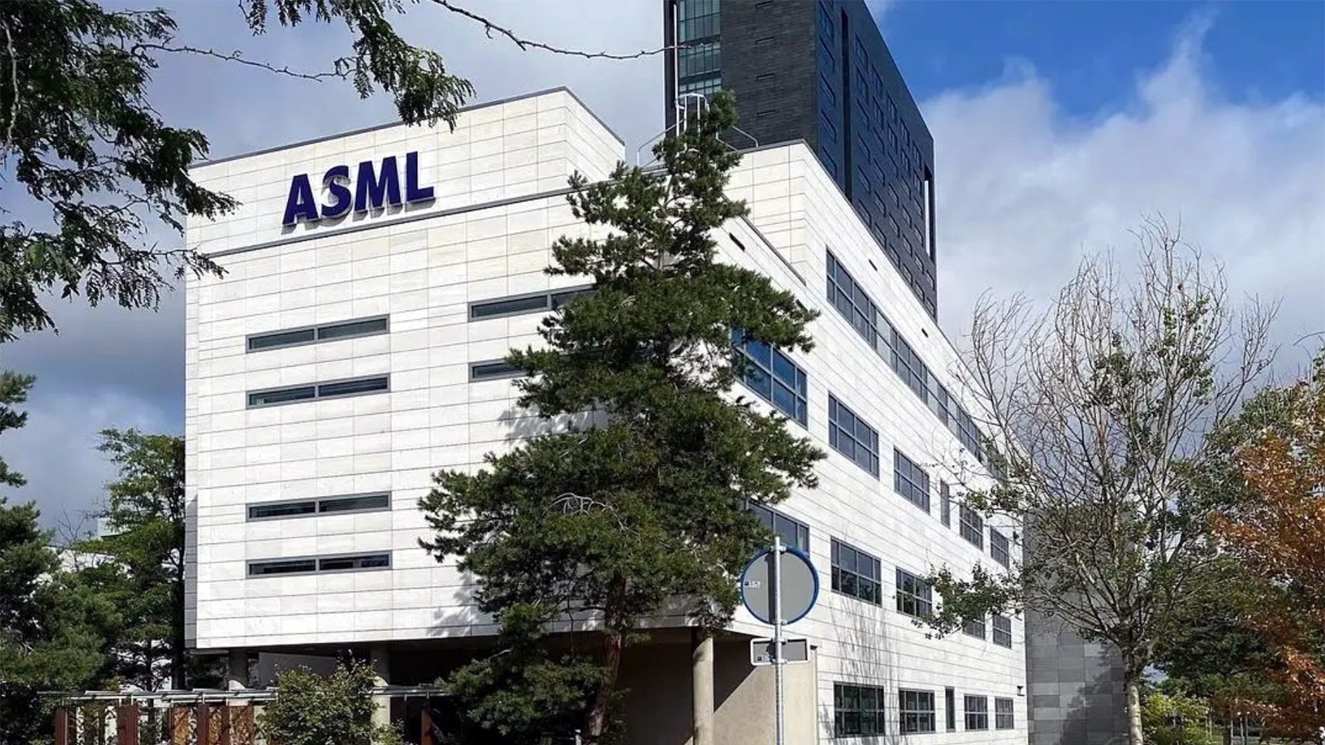
ASML, the undisputed leader in manufacturing these sophisticated tools, currently relies on laser-produced plasma (LPP) technology. This method involves firing powerful CO2 laser pulses at tiny droplets of molten tin, turning them into a plasma that emits the required EUV. The light is then meticulously collected by complex mirrors, all while fighting the inherent difficulty of operating in a vacuum using reflective optics—a necessity because virtually all materials absorb this high-energy radiation.
To keep pace with the demands of modern chip fabrication, ASML is steadily boosting the power of its LPP sources, increasing output from around 250W to 500W, and planning to reach 1000W in the coming years. Furthermore, the company is scaling up the production process by aiming to generate up to 100,000 tin droplets every second.
But there is a compelling alternative on the horizon: the free-electron laser (FEL). This technology bypasses the need for molten material entirely. Instead, a FEL accelerates electrons to near the speed of light and forces them through an undulator—a series of alternating magnets—causing them to emit light with the exact 13.5-nm wavelength needed. This method promises the elimination of tin droplets and associated debris, potentially offering substantially higher EUV power from a single source.
However, the path to the FEL is paved with monumental engineering obstacles. While the result sounds theoretically cleaner, creating a functional FEL demands an incredibly complex system. It requires a full particle accelerator, an electron source, extensive radiation shielding, precise beam control, and highly sophisticated mirror systems capable of handling massive amounts of EUV power without losing efficiency.
The fundamental hurdle is that the FEL approach demands semiconductor fabrication levels of availability, efficiency, and cost—standards that took the industry years to achieve. This complexity means that while enthusiasm surrounds the FEL in key regions like China, the U.S., and Japan, the timeline for true competitive parity remains long. Experts suggest it will likely take a decade, if not more, before FEL technology can match the practicality of LPP in real-world semiconductor production facilities. The race for the perfect EUV light source is not just a scientific endeavor; it is a complex engineering marathon.
Buy on Amazon
Credit