
Samsung Foundry targets 1nm nodes by 2030 using High-NA EUV
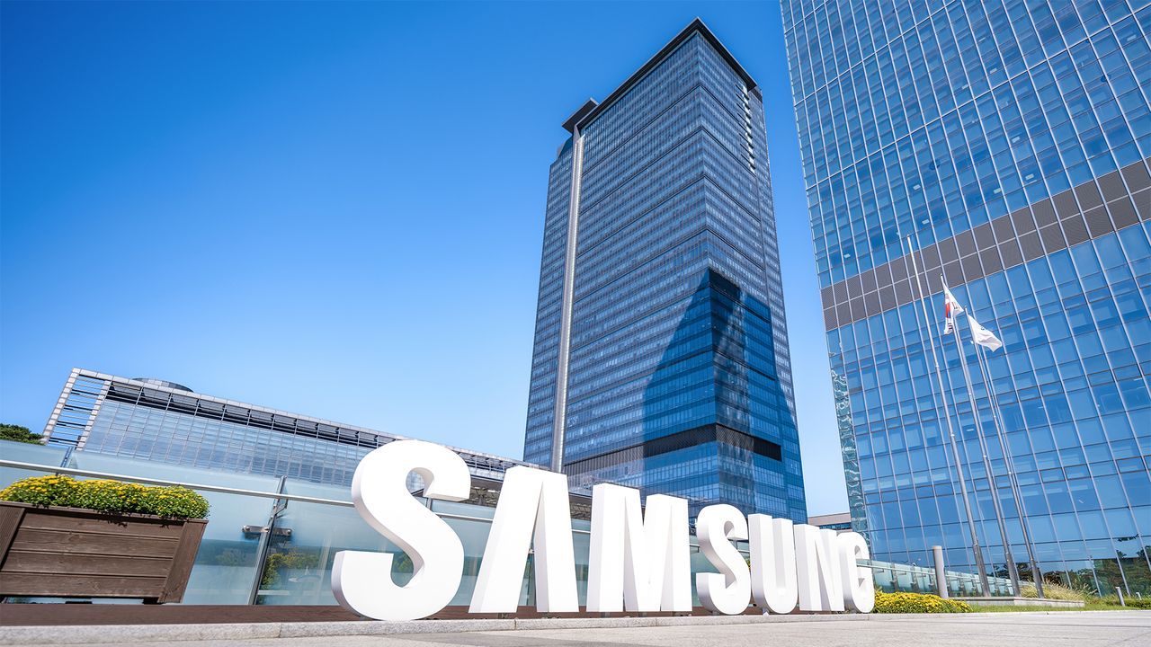
Samsung Foundry Rewrites the Roadmap: The Race for Next-Gen Chip Fabrication
The world of semiconductor manufacturing is constantly accelerating, and at the heart of this race lies Samsung Foundry’s ambitious new fabrication roadmap. At the recent Next-Generation Lithography + Patterning Conference (NGL 2026), Samsung unveiled significant shifts in its technological approach, signaling a strategic pivot designed to maximize competitiveness and ensure supply for the era of advanced AI chips.
Instead of rushing the market with its current 1.4nm-class technology, Samsung is opting to focus intently on refining its SF2 (2nm-class) manufacturing processes over the next three years. This decision reflects a pragmatic acknowledgment that achieving true commercial viability—measured by yields and volume—is paramount in the highly competitive foundry landscape.
This strategic pause is not merely a delay; it’s a calculated move to ensure that Samsung’s most advanced nodes are commercially robust. The company is taking time to hone the SF2 family, which includes processes like SF2P, SF2X, SF2A, and SF2Z, alongside incorporating innovative features such as backside power delivery.
Looking ahead, Samsung plans to introduce its 1.4nm-class process in 2029, building upon the refined SF2 foundation. A key component of this evolution involves introducing the SF1A (1nm-class) fabrication node, which will be the first to adopt High-NA EUV lithography tools.
This move introduces an interesting duality: Samsung is positioning itself with both an innovative 1nm-class process utilizing High-NA EUV and an enhanced SF1.4+ technology that relies on proven Low-NA EUV flows and materials. This layered approach allows the company to leverage established technologies while pushing the boundaries of next-generation patterning.
Despite having access to cutting-edge tools, such as ASML’s Twinscan EXE:5000 EUV scanner, Samsung is not prioritizing immediate mass adoption of High-NA EUV for its 2nm and 1.4nm technologies. The company maintains that these advanced tools still require further refinement before full implementation.
“We wanted to apply High-NA EUV to mass production at nodes such as 2nm and 1.4nm, but the technology still requires further improvements,” stated Chang Min Park, Master VP of Technology at Samsung Electronics. He noted that true High-NA EUV capabilities will likely become necessary for nodes at A10 and below, and the company is actively engaged in joint development with partners to achieve this goal.
The industry grapples with the practical challenges of High-NA EUV adoption. The systems involve substantially higher costs than current Low-NA systems, which directly impacts the overall cost of fabrication and chip production. Furthermore, implementing a smaller exposure field requires complex solutions like die stitching and demands significant improvements in photoresists, masks, and metrology.
Ultimately, the future of lithography hinges on finding the right balance between performance and practicality. While competitors like Intel are integrating High-NA EUV into some of their 14A technologies, Samsung’s phased approach suggests a methodical path. By focusing on perfecting the SF2 family first, Samsung aims to ensure its next generation of chips is not just technically advanced, but also commercially competitive.
Buy on Amazon
Credit