AI’s race for photonic interconnects and scale
The Light Race: How AI is Rewiring the Future of Computing
For years, the race for superior AI hardware focused on traditional metrics: raw processing power, memory capacity, and clock speeds. But as hyperscale data centers push boundaries, a new bottleneck has emerged—the fabric connecting those powerful chips. This invisible layer, the interconnect, is now dictating whether AI hardware can truly follow the principles of Moore’s Law or break out into an entirely new paradigm.
The key to unlocking this performance lies not just in packing more silicon, but in mastering networking. As experts point out, the true limitation on AI system performance is how quickly and efficiently data can travel across complex systems. Achieving high-performance AI requires solving three interconnected problems: Scale-up (internal server communication), Scale-out (cluster connectivity), and Scale-across (linking entire data centers).
The historical reliance on copper wiring has reached its limit. While sufficient within a single server, the physical reach and supply constraints of copper have created a wall for larger AI systems. This realization is driving a radical shift toward optical interconnects—using light to transmit data—to achieve the low latency and massive bandwidth essential for modern AI.
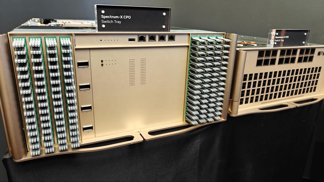
This technological evolution involves moving light closer to the processing itself. The journey has progressed from traditional pluggable transceivers, which sit a distance away, toward near-package optics. The next major step is co-packaged optics (CPO), where optical chiplets are integrated directly onto or beneath the GPU and switch. Each leap forward in this integration promises greater speed and reduced energy consumption.
The economics of this shift are compelling. While networking consumes a significant portion of data center energy, experts note that even with dramatic energy savings from optics, the sheer demand for AI hardware means the pursuit remains focused on fitting more compute, often needing to stick another 1,000 GPUs into the system.
In this rapidly evolving landscape, a standards war is brewing. While Nvidia has established a dominant position with its integrated solutions like NVLink and Spectrum-X, competitors are aggressively pursuing alternative interconnects. This competition involves defining new optical specifications and architectures, such as AMD’s UALink layered over Ethernet, challenging the traditional playbook.
The debate centers on different approaches to implementation: co-packaged optics (CPO) versus linear-drive pluggable optics (LPO). While CPO offers superior power efficiency by integrating lasers directly with the chip, LPO maintains greater modularity and serviceability. Experts predict that both technologies will coexist, split by application, though one path is likely to dominate based on specific AI workloads.
Ultimately, the foundation of this entire revolution hinges on light itself. Silicon is brilliant for electronics but struggles to emit light. The challenge now is mastering the process of turning silicon into an efficient light source. This bottleneck is where the industry’s greatest economic opportunity lies, and where ensuring a resilient supply chain for critical laser components becomes paramount.
Major players are responding by establishing industry-wide standards, such as the Optical Compute Interconnect (OCI) Multi-Source Agreement, aiming to define a common optical physical layer for AI infrastructure. This collaborative effort seeks to ensure that as we build the next generation of AI clusters, the ability to connect them with blazing speed and efficiency is guaranteed.
Buy on Amazon
Credit