CPO Foundry Roadmaps: Breaking Down TSMC, Intel, Samsung Strategies
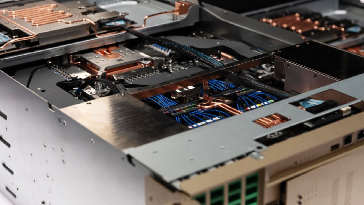
The relentless march of Artificial Intelligence is running headlong into a formidable wall: connectivity. As AI clusters demand ever-increasing bandwidth, the traditional electrical links that power data centers are proving to be the bottleneck. To feed thousands of accelerators efficiently, the industry is no longer looking for incremental upgrades; it is demanding an exponential leap in communication infrastructure.
The solution lies in Co-Packaged Optics (CPO)—a revolutionary shift where optical interfaces move from external modules to directly integrated components near the processor itself. This evolution is not just a technical tweak; it’s a fundamental re-architecture of how computing power communicates, pushing optical connectivity closer to the silicon heart of the machine.
For decades, relying on electrical links has been the standard. However, as signaling speeds climb past 200 Gb/s and beyond, transmitting data over long copper traces becomes increasingly inefficient, demanding complex circuitry, higher power consumption, and stricter signal integrity requirements. This limitation means that even the fastest processors are constrained by their physical wiring.
CPO addresses this inefficiency head-on. By placing optical engines next to the CPU or switch ASIC, CPO dramatically shortens the electrical path signals must travel before converting them into light. This approach promises lower power consumption per transmitted bit, vastly increased bandwidth density, and predictable scalability—all essential traits for next-generation AI infrastructure.
The race to implement this future is currently defined by the strategies of the world’s leading semiconductor foundries, who are collectively pioneering distinct paths toward making CPO ubiquitous. Intel, TSMC, Samsung Foundry, and GlobalFoundries are each developing unique approaches to embed light into the silicon ecosystem.
TSMC is charting a detailed course with its Compact Universal Photonic Engine (COUPE) roadmap. This strategy involves three ambitious stages: starting with COUPE on PCB for 1.6 Tbps bandwidth, moving to COUPE on substrate integrating with chip-on-wafer-on-substrate (CoWoS) packaging, and finally, aiming for COUPE on interposer—integrating a 12.8 Tbps optical engine directly into the processor package. This progression aims for 5x power efficiency compared to current solutions.
Intel is pursuing a focus on the Optical Compute Interconnect (OCI) chiplet. Intel’s strategy centers on creating self-contained optical I/O subsystems that pack electronic and photonic components alongside compute devices, allowing optical connectivity to be integrated directly with CPUs, GPUs, and accelerators through technologies like PCIe. While their initial prototype demonstrated 4 Tbps of bandwidth over fiber pairs, the focus remains tightly bound to integrating optics with compute elements.
Samsung Foundry appears to have adopted the most comprehensive strategy, aiming to provide a full spectrum of optical solutions. Their plan involves offering merchant pluggable transceivers first, followed by intermediate technologies like thermo-compression bonding (TCB) for integrating optical engines on substrates. By 2028, Samsung aims for true CPO by placing optical engines on switch ASIC substrates and eventually on the processor interposer, striving for an ultimate turnkey solution by 2030.
GlobalFoundries offers a vendor-agnostic approach through its SCALE platform, designed to become a merchant Co-Packaged Optics provider. Their focus is on enabling optical connectivity (OCI MSA) for processors made by any chipmaker. By allowing clients to customize their optical engines while maintaining compatibility with industry standards, GlobalFoundries aims to provide the flexible backbone necessary for mass adoption across the AI data center.
Ultimately, these divergent foundry roadmaps all converge on a single goal: moving optical interfaces closer to compute dies. Whether through specialized engine development or integrated chiplets, the collective objective is clear—to redefine the architecture of AI infrastructure by maximizing bandwidth density, slashing power consumption, and drastically lowering latency for the future.
Buy on Amazon
Credit
