Custom HBM promises 30% bandwidth and 15% power gains
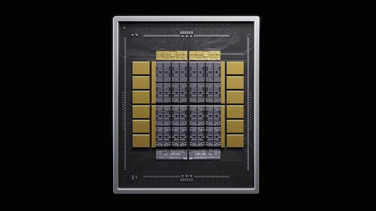
Nvidia Unleashes NVHBM: Redefining the Rules of AI Infrastructure
The race to build the next generation of artificial intelligence infrastructure is defined by one fundamental challenge: how to move data fast enough. As AI models grow exponentially, the bottleneck has shifted from raw processing power to the sheer capacity and speed of data movement. To tackle this monumental task, Nvidia is not just optimizing chips; they are introducing revolutionary building blocks that promise to unlock unprecedented performance in the AI era.
At the heart of this innovation is the NVLink Fusion program, a framework designed to connect custom chips with the high-speed NVLink domain, enabling the creation of coherent, massive-scale systems like the Vera Rubin accelerator. Now, Nvidia is adding a critical new component to this toolkit: NVHBM, a custom implementation of high-bandwidth memory that is poised to redefine how AI accelerators operate.
NVHBM is more than just faster memory; it is a custom solution engineered specifically for the demands of AI. By integrating this memory directly with the custom silicon, Nvidia is achieving a trifecta of advancements: significantly higher bandwidth, dramatically reduced power consumption, and a smaller physical footprint on the accelerator die.
For workloads that are memory-bandwidth-bound—which is the reality for massive AI calculations involving model weights and key-value caches—these improvements translate directly into tangible gains. NVHBM offers up to 30% higher bandwidth per stack than conventional HBM4e. This means that AI inference can achieve higher tokens-per-second rates, drastically accelerating the pace at which complex models can deliver results.
Beyond raw speed, the efficiency gains are equally compelling. Traditional approaches often waste energy on data movement. NVHBM cleverly moves the memory controller into the base die of the HBM stack, simplifying the overall design and freeing up valuable real estate on the main custom accelerator chip. This architectural shift allows designers to allocate up to 30% more compute die area to actual processing, rather than memory circuitry.
Furthermore, energy efficiency is paramount. Nvidia reports that NVHBM consumes 15% less power than off-the-shelf HBM4e. This energy savings is crucial, allowing performance-per-watt improvements that can be reinvested directly into enhancing the accelerator itself, or supporting a larger number of processing units within the same power budget.
This strategic focus on efficiency and density is not just theoretical; it is becoming the practical foundation for future AI systems. The ability to move vast amounts of data with less energy means that cutting-edge AI systems can operate more sustainably and deliver superior performance in real-world deployments.
The impact extends beyond Nvidia’s immediate ecosystem. This technology is already finding strong allies. Amazon’s Annapurna Labs is stepping up as a first partner for NVHBM, signaling a collaborative effort to enhance future AWS infrastructure designs. As hardware progresses, it is clear that this integration of custom memory and custom interconnects is the essential building block for the next era of high-performance, energy-efficient AI computing.
Buy on Amazon
Credit