DIY LED maker uses bathroom laser for sapphire etching
Forget sterile factory floors and multi-billion dollar foundries; some of the most revolutionary advancements in semiconductor technology are now being born right in the backyard. A dedicated hobbyist is turning a garden shed into a cutting-edge laboratory, proving that the next generation of microchip innovation doesn’t require a corporate budget, only ambition and a deep understanding of physics.
Matthew Hartensveld is leading this charge, transforming his space into a personal cleanroom where he is fabricating his own RAM memory cells. The project, part of his open-source Semiconductor.DIY initiative, is less about following industry blueprints and more about hands-on discovery, pushing the boundaries of what is achievable with DIY technology.
The initial challenge was impressive. Hartensveld began by setting up his environment, using gallium nitride atop a sapphire wafer. To prepare the material for etching, he followed rigorous cleaning protocols, using a mix of deionized water, acetone, and isopropyl alcohol to ensure a pristine surface.
To define the essential patterns required for the memory cells, he faced a classic etching dilemma. While industrial processes rely on hazardous chlorine gas, Hartensveld sought a safer, more accessible solution. He moved to the next great challenge: transforming the raw material into light. He turned his attention to household lasers, seeking to use them for etching and patterning.
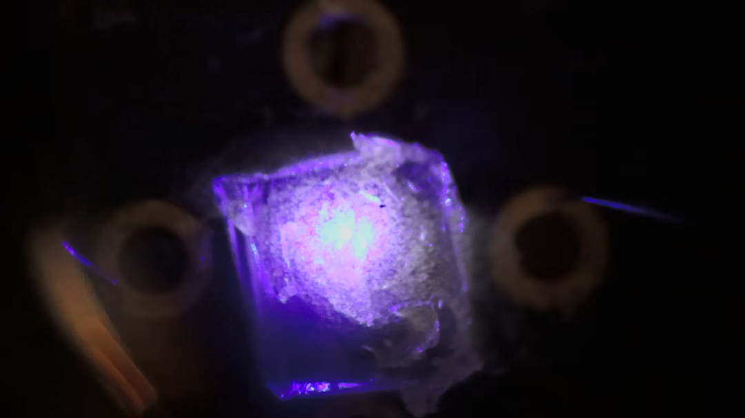
After experimenting to discover the right etching method, he managed to etch patterns onto the wafer. The real magic, however, occurred when he experimented with turning these etched shards into light sources. By depositing indium and applying a battery, he achieved a working blue light—a color that remained a decades-long mystery to dedicated engineers.
To refine the process, Hartensveld employed extreme precision. He used a vacuum chamber with a two-stage pump to remove nearly all residual air, then deposited specialized layers of nickel/silver and titanium/silver for the positive and N-contacts. This was followed by an argon plasma treatment, ensuring a clean, functional connection.
The next hurdle was packaging these discoveries. Traditional methods failed, so Hartensveld reverted to the laser, using it to precisely melt away the sapphire substrate, effectively cutting the memory cells into usable pieces. For the physical connections, he opted for indium bumps, a method familiar from digital camera technology.
The final, whimsical touch involved finishing the electrical package. To achieve a more practical, visible light source, he added a layer of cerium-doped yttrium aluminum garnet, creating a yellow filter that transformed the raw output into a functional, albeit wonderfully imperfect, white LED. This journey demonstrates that with open-source knowledge and sheer determination, the future of semiconductor manufacturing is truly free-range.
Buy on Amazon
Credit