Google’s ‘Frozen v2’ chip uses Gemini for 10x more tokens per watt than TPUs
The Future is Etched In: Google’s Radical Plan to Build AI Directly into Silicon
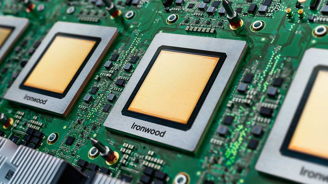
The race for smarter artificial intelligence is running on two tracks: increasing model complexity and radically increasing computational efficiency. At the intersection of these demands, a major tech giant is pushing the boundaries of hardware design, not just by making existing chips faster, but by rethinking how AI itself runs. Google is quietly developing a groundbreaking server chip, informally known as “Frozen v2,” that aims to etch parts of its powerful Gemini model’s architecture directly into the silicon—a move designed to redefine the limits of AI processing.
This isn’t just an incremental update; it’s a fundamental shift in how large language models interact with hardware. Current systems, relying on traditional setups like TPUs, require complex runtime decisions as data shuttles around the chip. Frozen v2 seeks to eliminate much of this overhead by baking critical model decisions directly into the transistors themselves. The result? Engineers project that this approach could deliver six to ten times more tokens per unit of power than the newest generation of Google’s custom accelerators.
The immediate payoff for such efficiency is staggering. By minimizing the steps and data movement required per query, Frozen v2 promises to drastically cut response latency. This reduction in delay could unlock entirely new applications, allowing AI systems to operate with the speed and responsiveness needed for truly real-time interaction.
While some visions of this future have already been explored—including proposals to permanently bake model weights into the chip—Google’s “Frozen v2” takes a pragmatic, evolutionary approach. Instead of locking down the architecture entirely, the new chip freezes the structure while keeping the weight data updatable. This ensures the hardware remains useful across successive Gemini releases, making it an adaptable and long-lasting solution for evolving AI demands.
This initiative is driven by a clear market reality. The severe global AI compute shortage has already forced major players like Google Cloud to turn down external customer deals, highlighting the critical need for internal, hyper-efficient solutions. Frozen v2 represents a strategic effort to maximize the utility of existing silicon and prepare for an imminent need for extreme computational power.
Google doesn’t plan on replacing its existing TPU line but views this specialized chip as part of a broader strategy: splitting hardware into dedicated training and inference variants. This approach positions Frozen v2 to sit alongside other advanced silicon solutions, allowing it to integrate seamlessly into the evolving data center landscape rather than disrupting it.
The ambition behind this project is matched by the timeline. Google is targeting deployment for this specialized silicon as soon as 2028. This timeline aligns with massive industrial movement, including reports that Google has reportedly booked over three million TPUs from Intel for the same year, signaling a massive investment in AI infrastructure across the industry.
The quest for efficiency extends beyond Google’s labs. Other innovators are already pursuing similar avenues. Startups are demonstrating model-hardwired inference silicon, achieving high token throughput with minimal memory usage, and major players like Nvidia are finalizing enormous deals to license core technology from specialized chip designers. The movement is clear: the future of AI compute demands hardware that thinks just as fast as the algorithms they execute.
Though Google remains cautious about public production details, emphasizing that this rigorous exploration is central to their full-stack approach, the work being done with Frozen v2 signals a powerful trajectory. It’s an ambitious blueprint for how we will move from theoretical AI models to truly instantaneous, energy-efficient, and ubiquitous intelligence.
Credit
