Intel chips dual-qualified by ASML’s High NA EUV
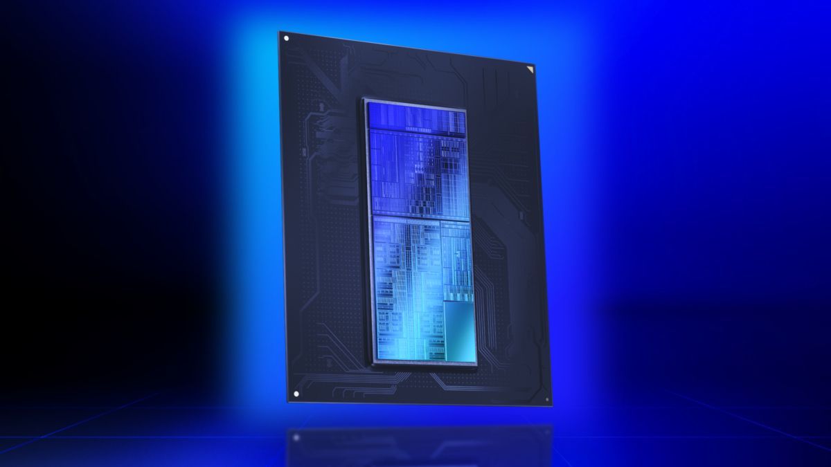
The race for smaller, faster processors is constantly accelerating, but this time, the leap in chip manufacturing technology has truly changed the game. Intel has made history by entering high-volume manufacturing using ASML’s cutting-edge High NA extreme ultraviolet (EUV) lithography technology for select components of its Core Ultra Series 3 “Panther Lake” processors.
This achievement positions Intel as the first company to ship high-volume logic products utilizing this advanced technique. The milestone was officially confirmed by ASML, highlighting the successful operation of the High NA layers on Intel’s 18A process node in Oregon.
What makes this breakthrough so significant is the technology itself. High NA EUV is the successor to current EUV lithography, designed to dramatically extend semiconductor scaling. By increasing the numerical aperture—the amount of light a lens can focus onto a silicon wafer—from 0.33 to 0.55, manufacturers can resolve finer features with greater precision in a single exposure.
This enhanced resolution allows chipmakers to print smaller, denser circuit patterns, which is crucial for meeting the demands of increasingly complex designs. This capability promises to reduce reliance on complicated multi-patterning techniques, simplifying manufacturing while simultaneously boosting feature fidelity.
Rather than an outright replacement of the entire fabrication flow, Intel is employing High NA EUV strategically. They are applying it only to specific layers within their process, allowing the rest of the chip to continue using conventional lithography methods. This flexible approach maximizes efficiency and leverages existing infrastructure while pioneering the use of next-generation technology.
ASML President and CEO Christophe Fouquet noted that this development is key to enabling the smaller, denser patterning required to accelerate advancements in fields like AI. “We are proud to play a role in enabling the smaller, denser patterning that will accelerate advancements in AI and other emerging technologies,” he stated.
Intel’s journey to this point involved years of focused research and development. The company successfully installed industry-first commercial High NA EUV lithography systems, including ASML’s second-generation TWINSCAN EXE:5200B. This work ensures that the high-volume wafer flow is not only cutting-edge but also delivers consistent yields for customers.
While the initial focus was on optimizing the Intel 18A process node, this milestone sets the stage for future evolution. The flexibility gained allows Intel to adapt this technology for future nodes, such as the planned Intel 14A process, where High NA EUV can be used to handle the tightest-pitch layers, further pushing the boundaries of processor performance and density.
Buy on Amazon
Credit