Intel EMIB bypasses TSMC CoWoS for Google TPUs
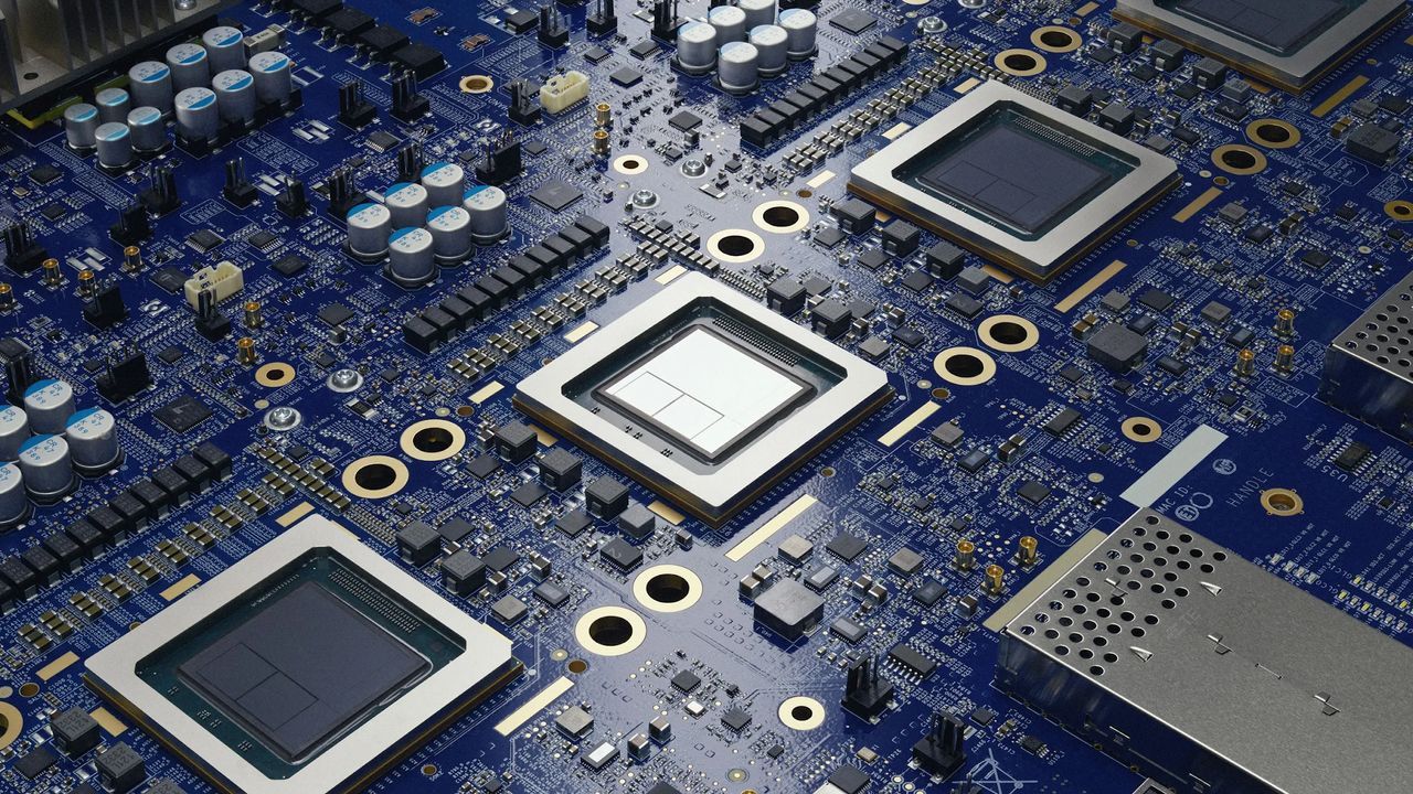
The race for the next generation of AI hardware isn’t just about faster processors; it’s a high-stakes architectural showdown fought on the silicon package itself. At the center of this battle is Google’s decision regarding how to pack its massive Tensor Processing Units (TPUs). The choice—between the established standard and an innovative challenger—could redefine the future of AI accelerator design.
For years, the industry has anchored itself around TSMC’s CoWoS technology as the gold standard for advanced packaging. This chip-on-wafer-on-substrate approach has been the go-to solution for nearly all cutting-edge AI and High-Performance Computing (HPC) processors, including Google’s various generations of TPUs.
Now, the landscape is shifting. Google is reportedly exploring an alternative: Intel’s Embedded Multi-Die Interconnect Bridge (EMIB-T) packaging for its upcoming Ninth-Generation TPUs, codenamed Humufish. This move signals a potentially dramatic pivot, trading one established method for another complicated endeavor that promises both technical breakthroughs and significant strategic shifts.
To understand the appeal of this switch, we must look at the technology itself. The current CoWoS architecture utilizes Redistribution Layer (RDL) interposers with embedded silicon links to manage high-density communication across large dies. In contrast, Intel’s EMIB-T embraces a fundamentally different approach. Instead of relying on bulky interposers, EMIB-T uses tiny embedded silicon bridges within the organic substrate to facilitate die-to-die connections.
This difference is crucial for power delivery. The EMIB-T design incorporates advanced features like through-silicon vias (TSVs) for vertical power flow and integrated metal-insulator-metal (MIM) capacitors directly into the bridges, which dramatically improve power integrity—a vital necessity for powering sophisticated AI accelerators.
While the argument that EMIB-T offers freedom from reticle limits is compelling, the true advantage lies in specialized functions. CoWoS-L excels at package-wide routing density, providing flexible routes across large areas. EMIB-T, however, focuses on local interconnection density, achieving incredibly dense links between adjacent dies. It’s a trade-off between global flexibility and local efficiency.
The choice ultimately boils down to balancing technical performance with real-world constraints. While CoWoS-L offers predictability based on existing industrial experience, EMIB-T presents potential gains in mechanical rigidity by eliminating large interposers, although managing the complex stresses introduced by vertical structures is Intel’s challenge.
Beyond the physics of packaging, the economics play a significant role. By exploring EMIB-T, Google may be looking to mitigate supply chain risks associated with TSMC’s constrained CoWoS capacity. Furthermore, this exploration could open new strategic doors, allowing Google to build relationships with Intel Foundry and diversify its chip supply chain.
Ultimately, whether the path leads through TSMC’s established framework or Intel’s novel approach depends on a delicate balance of technological capability, mechanical demands, and long-term business strategy. It is an exciting time for advanced packaging, where the next great leap in computing may be defined by a daring new design.
Credit
