Intel leads EUV processing and unveils new production masks
The Lithography Leap: How Intel is Redefining the Future of Chipmaking
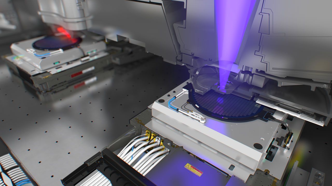
In the relentless world of semiconductor manufacturing, where every nanometer counts, Intel is charting a course toward a monumental milestone. The company recently announced that it has processed more than one million 300-mm wafers using its High-NA EUV scanners—a feat achieved in less than two and a half years since the first tool was assembled. This achievement is more than just a processing number; it represents a significant leap in operational maturity for the entire industry.
This impressive figure incorporates wafers processed during tool installation, certification, research and development, and full production. As Intel expands its fleet of tools, including the EXE:5200B scanner alongside its EXE:5000 systems, the million-wafer mark signifies a critical inflection point in process development. In fact, this cumulative utilization by Intel far outstrips the rest of the industry combined, demonstrating a pioneering level of High-NA tool application.
But the real challenge lies in how this technology translates into physical chip design. Current limitations mean that even with High-NA EUV, chip designers still face complexity. Conventional exposure methods often necessitate a technique called stitching, where large dies are split into two half-fields for exposure. This approach, while workable in the near term, introduces significant friction into the manufacturing process.
Stitching comes with tangible costs. It dramatically reduces throughput—slowing production from 175 wafers per hour down to 125 wafers per hour on some tools. Furthermore, chip architects must design layouts with stitching in mind, sacrificing freedom in floor planning. Most critically, achieving perfect alignment across the stitching boundaries is an exercise in extreme precision. Even slight misalignment can introduce defects, distorting critical lines and interconnects, posing a costly risk for complex CPU and GPU dies.
To eliminate these inefficiencies, the industry is pivoting toward a radical solution: larger photomasks. The goal is to shift from the familiar 6-inch mask format to massive 6×12-inch masks, which would allow High-NA EUV scanners to expose the entire 26×33 mm field in a single exposure, eliminating the need for stitching entirely.
This transition, however, is not merely a change in mask size; it represents an overhaul of the entire semiconductor ecosystem. Moving to 6×12 masks necessitates substantial changes across every stage of the supply chain, including mask blanks, deposition, etching, inspection, and handling systems. The High-NA EUV scanners themselves would also need redesigns to accommodate these larger formats.
While the exact timeline for this revolution remains unfolding, Intel is positioning itself as a powerful catalyst for change. If the industry successfully adopts this larger mask standard, Intel stands to gain a significant first-mover advantage, setting the foundational rules for the projection lithography infrastructure for decades to come.
Buy on Amazon
Credit
