Nvidia CEO: China will have advanced chipmaking tools by 2030
The global race for technological supremacy is increasingly defined by access to advanced manufacturing tools. While nations are pouring vast resources into self-sufficiency, a critical bottleneck remains in the heart of the semiconductor industry: the lithography tools required to etch the future of microchips.
China’s progress in developing advanced technology is undeniable, yet there is one area where the nation has fallen significantly behind global leaders. The sophisticated lithography systems offered by companies like ASML currently set the global standard, and matching this capability has long been a major hurdle for the domestic semiconductor industry.
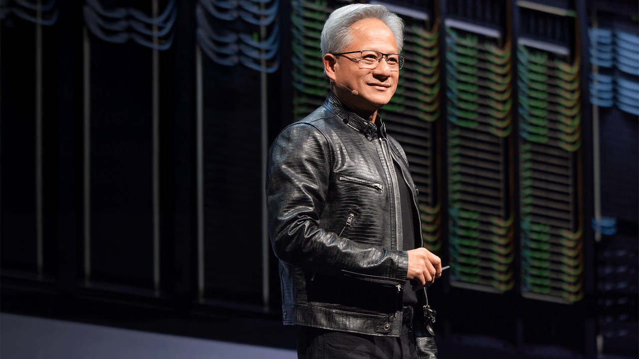
Despite this gap, optimism persists. Industry leaders believe that rapid investment and focus will close the divide. For instance, Nvidia CEO Jensen Huang suggests that China will develop its own advanced lithography systems within just three or four years, setting the target for 2030.
“They are going to get there by 2030,” Huang stated, suggesting that China’s strength lies in high-volume production, implying that catching up on cutting-edge tools is merely a matter of time.
However, bridging this gap is not a simple matter of replicating existing technology. China has made strides in dry scanning, with companies like Shanghai Micro Electronics Equipment capable of mass-producing 193-nm ArF scanners. They have also developed immersion scanners capable of handling 28-nm-class processes. Yet, the challenge shifts from merely developing a prototype to achieving high-volume, production-quality manufacturing.
Realizing the potential of these tools requires more than just delivery; it demands mastery of complex engineering. Even if initial scanners are delivered in the coming years, widespread deployment for high-volume chip production will likely take several more years. Achieving parity with ASML’s contemporary systems remains highly unlikely by the 2030 deadline.
The challenge escalates dramatically when considering the next frontier: Extreme Ultraviolet (EUV) lithography. While reports indicate that Chinese scientists have made significant headway in developing the laser-produced plasma source needed for the 13.5-nanometer wavelength light, assembling a complete, production-ready EUV scanner introduces a far greater set of engineering complexities.
Developing EUV tools requires not only mastering the light source but also solving the hardest problems in alignment, projection optics, metrology, and wafer handling—the same challenges inherent in advanced DUV technology. If China is still struggling to industrialize the capabilities required for immersion DUV, the leap to EUV is an extraordinary feat. Despite the geopolitical stakes of the AI race, the journey to full lithographic self-sufficiency is a monumental engineering undertaking that demands extraordinary focus and ingenuity.
Buy on Amazon
Credit
