
Samsung debuts three next-gen memory techs for AI data centers
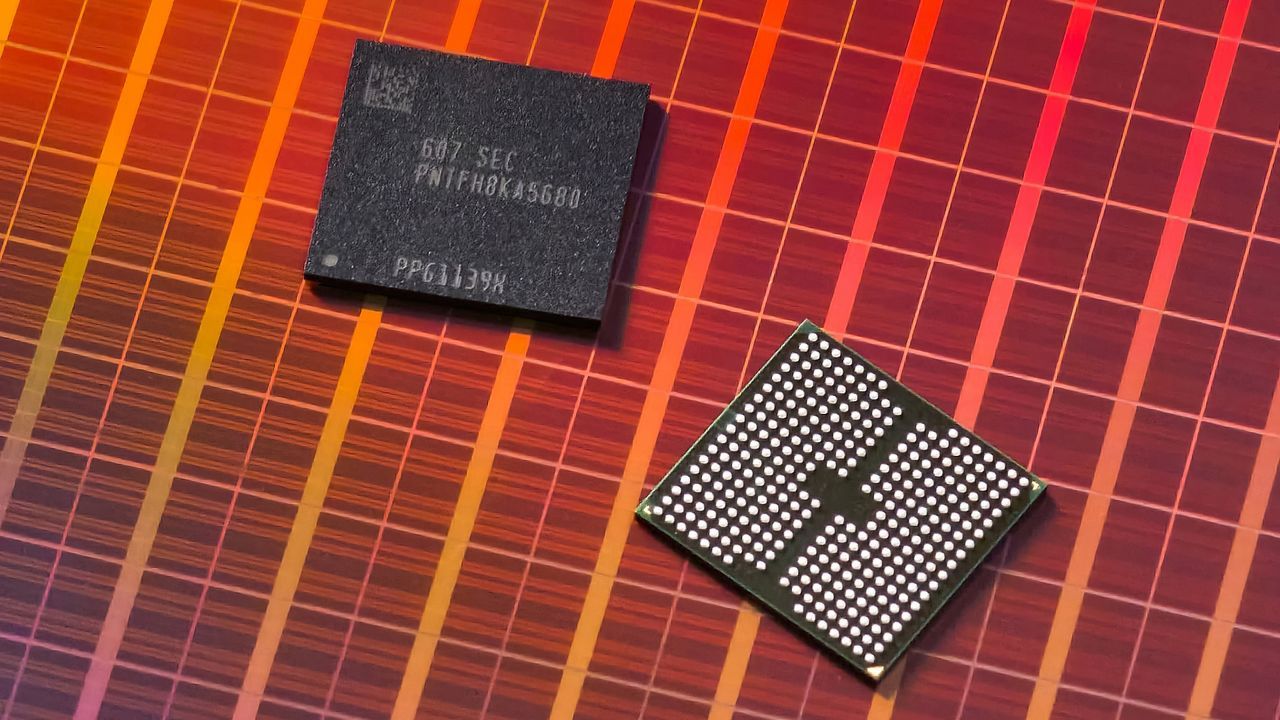
The world of semiconductor innovation is moving at warp speed, especially when it comes to memory and storage. At the recent Future of Memory and Storage (FMS) 2026 conference, Samsung didn’t just present new chips; they unveiled a radical vision for how memory will interface with computation, introducing technologies that promise to redefine the limits of data bandwidth and efficiency. The common thread running through these groundbreaking concepts—zHBM, zNAND-O, and BV-NAND—is a shared architectural principle: wafer bonding, pushing memory integration directly onto logic circuitry.
This approach aims to solve the fundamental bottlenecks in current computing architectures by eliminating the distance data must travel. By placing memory systems directly alongside or atop processors, these innovations are set to unlock unprecedented performance for AI accelerators and demanding general-purpose applications.
Take zHBM, for instance. This concept envisions stacking High Bandwidth Memory (HBM) directly on top of logic dies. By eliminating the traditional perimeter connection, Samsung aims to dramatically reduce latency and maximize bandwidth between the memory and the AI accelerator. The promise is huge: achieving approximately eight times the performance of HBM5 while also delivering up to ten times higher memory density and significantly improved energy efficiency compared to existing standards.
However, with such ambitious claims come the necessary engineering caveats. While the potential for denser and faster memory is undeniable, details remain open regarding the exact definition of ‘performance’ when comparing these new structures. The actual realized gains will depend heavily on complex factors like thermal management and the development of novel interconnects that can handle interfaces as demanding as 2048-bit systems.
Simultaneously, Samsung is revolutionizing storage with technologies designed to bring data closer to the compute. zNAND-O (on-device) seeks to achieve the same goal by bonding NAND memory atop logic devices. This minimizes latency and power consumption, making it an ideal candidate for real-time, data-intensive workloads in edge AI systems.
The evolution of 3D NAND itself is also taking a quantum leap with BV-NAND, or Samsung’s 10th Generation V-NAND. This new platform integrates the NAND array directly onto the I/O and logic wafer, enabling higher I/O speeds and enhanced density. With an areal density reaching 28 Gb/mm^2 and maximum I/O speeds up to 5600 MT/s, this technology provides a competitive edge in storage performance.
This shift also involves a new branding strategy. By launching technologies like BV-NAND under a fresh name, Samsung is positioning itself not just as a supplier of memory, but as an innovator setting the pace for data center-grade AI accelerators that demand storage with latency lower than that of traditional SSDs. While these immediate breakthroughs focus on next-generation components, the full rollout of solutions like zHBM and zNAND-O suggests a roadmap stretching into the late 2020s and early 2030s.
Credit