Samsung HBM5 hints at 4096-bit interface with double speed
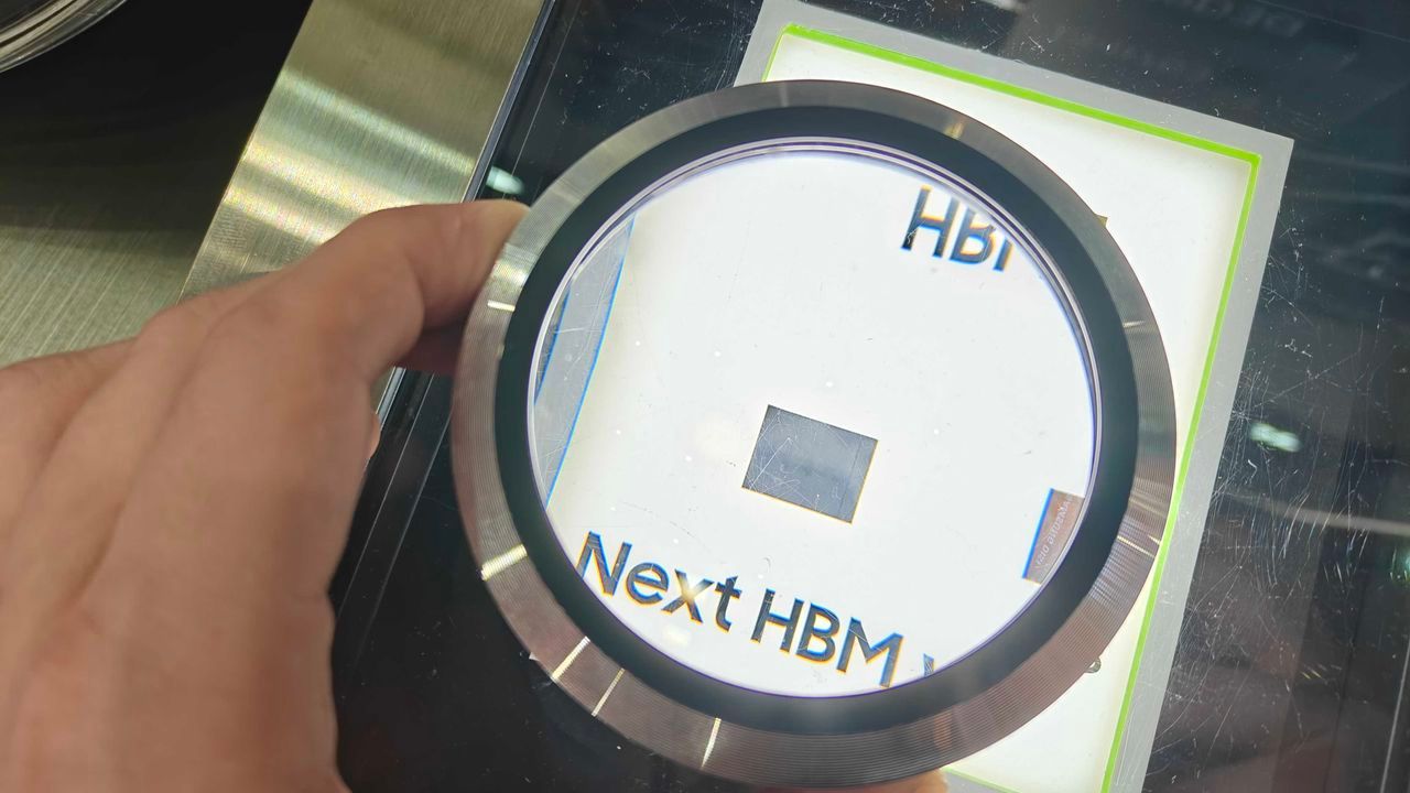
The quest for the next generation of High Bandwidth Memory (HBM) is pushing the boundaries of what silicon can achieve. As memory architects look toward HBM5, the goal isn’t just incremental improvement; it’s a massive leap designed to redefine performance and energy efficiency.
Samsung has set an ambitious target: HBM5 aims to double the performance and improve power efficiency by 20 percent compared to its predecessor, HBM4E. This ambitious vision is not just about faster chips; it involves fundamentally rethinking how data moves across the semiconductor landscape.
To make this jump in memory bandwidth realistic, engineers are grappling with colossal technical challenges. Doubling the data transfer rate in a single generation is a monumental task. This suggests that HBM5 will likely rely on increasing the number of interface pins to boost overall bandwidth, rather than simply increasing the speed of existing connections.
Samsung’s roadmap points toward peak performance figures in the coming years. If successful, HBM5 is projected to achieve peak memory bandwidths of around 4 terabytes per stack by 2028–2029. This capability will be critical for powering the massive demands of Artificial Intelligence and advanced computing.
The implications extend far beyond single stacks. Industry forecasts suggest that systems-in-packages leveraging HBM5/HBM5E could handle 20 to 24 stacks per package, translating to a staggering memory bandwidth of 80 terabytes to 96 terabytes just a few years down the line.
Achieving this bandwidth requires solving a complex physical engineering puzzle. Since current standards for HBM4E operate around 12 gigatransfers per second (GT/s), doubling the performance demands a radical change in interface design.
Engineers are weighing two primary paths to achieve this: either doubling the per-pin data transfer rate to 24 GT/s, doubling the interface width from 2,048 to 4,096 bits, or pursuing a combination of both.
While increasing the signaling speed to 24 GT/s is tempting, it introduces significant hurdles. Higher speeds demand more sophisticated drivers, receivers, clocks, and error correction mechanisms to maintain signal integrity, making the physical layer immensely complicated.
Conversely, widening the interface to 4,096 bits introduces another layer of complexity. This means doubling the number of Through-Silicon Via (TSV) and I/O paths, complicating routing, bump design, and base die manufacturing. While this method might offer better power-per-bit efficiency, the resulting package complexity could negate the performance gains.
Ultimately, the path to HBM5 success hinges on finding the optimal engineering compromise. Many experts suggest that a hybrid approach, perhaps combining a moderate increase in data transfer rate with an optimized interface width, might offer the best balance between raw speed and power efficiency.
It is important to remember that energy efficiency improvements, the other half of the HBM5 promise, are not solely dependent on bandwidth. Achieving a 20 percent boost in efficiency also relies on advancements in DRAM process technology, architectural optimizations, and sophisticated power management techniques. The future of high-performance memory is being written at the intersection of physics and engineering.
Credit