SK hynix breaks ground on US HBM plant for AI production in 2029
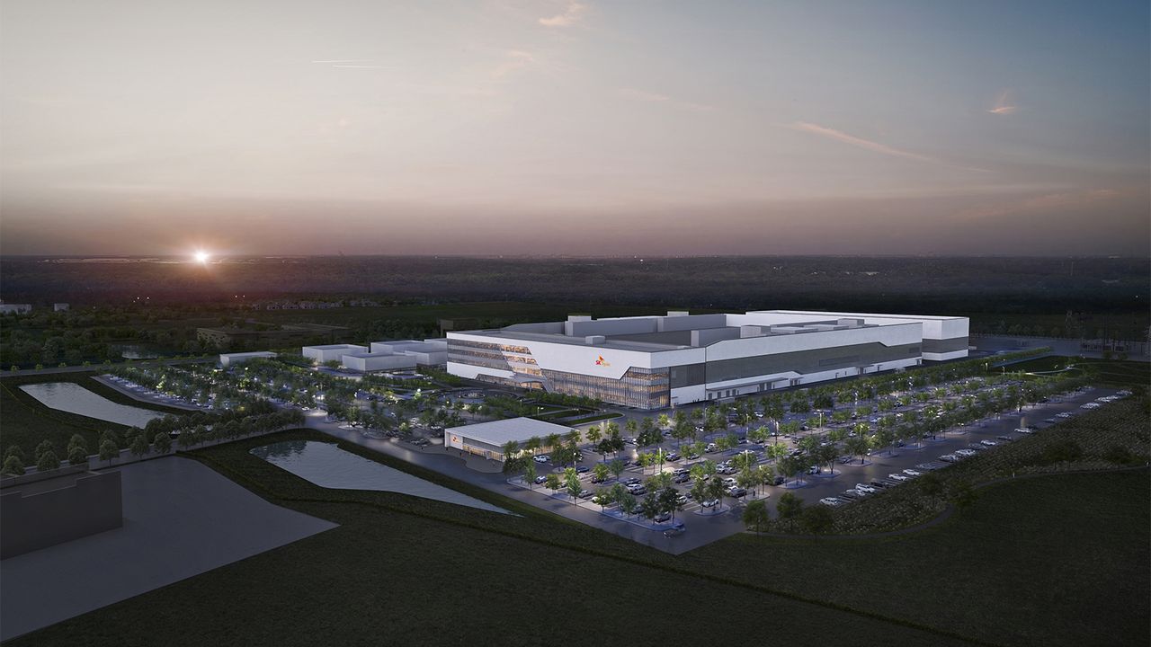
Building the AI Backbone: How Indiana is Becoming the Hub for America’s Next-Generation Memory
The race for artificial intelligence is fueled by memory, and at the heart of modern AI systems lies high-bandwidth memory, or HBM. While this crucial component drives the performance of next-generation computing, the assembly of these complex memory modules has historically been concentrated elsewhere. Now, a monumental shift is underway, positioning the United States to play a pivotal role in the semiconductor supply chain, specifically through a massive investment in Indiana.
SK hynix is pioneering this change by initiating the packaging of HBM memory modules at its new facility in West Lafayette, Indiana. This move isn’t just about building a factory; it’s about establishing a crucial domestic link for the advanced technologies needed to power the AI revolution. The company recently held a groundbreaking ceremony, signaling the start of construction for what is set to become a $4 billion hub for advanced semiconductor packaging.
This Indiana base will be the central location for advanced packaging, testing, and research dedicated to HBM. While the facility will not manufacture the underlying DRAM wafers—which are sourced from South Korea—it will perform the complex and highly specialized work of packaging HBM stacks. This facility is poised to make SK hynix’s resulting devices among the first truly “Made in USA” HBM products, giving American customers a competitive edge in the burgeoning AI market.
The timeline for this ambitious project is clear and focused. The company expects to open its cleanroom by October 2028 and begin volume production of next-generation HBM in the second half of 2029. This accelerated schedule demonstrates a commitment to bringing cutting-edge technology to fruition rapidly.
Beyond mass production, the facility is designed to be a dynamic center for innovation. SK hynix will establish an Advanced Packaging R&D Testbed alongside the manufacturing lines. This space will serve as an incubator, allowing the company to collaborate with customers, universities, and commercial partners to develop future packaging technologies, rapidly validate prototypes, and push the boundaries of manufacturability.
This collaborative approach is further solidified by strategic academic partnerships. SK hynix has signed a memorandum of understanding with Purdue University to jointly research system integration and advanced packaging technologies, further embedding the Indiana facility within the broader American research ecosystem.
As Kwak Noh-Jung, CEO of SK hynix, stated, this regional focus represents more than just manufacturing capacity. He emphasized that the United States is the epicenter of AI innovation, and this Indiana fab will serve as a vital gateway for delivering American-made HBM solutions. It is a commitment to growing together and becoming the most trusted partner in shaping the future of AI in America.
The establishment of this facility underscores a powerful trend: that leading-edge semiconductor technology is evolving into a highly integrated field. By focusing on advanced packaging and R&D within the U.S., SK hynix is not only manufacturing the future of memory but is actively creating a domestic ecosystem ready to lead the next wave of AI development.
Buy on Amazon
Credit