SK hynix pushes hybrid bonding to HBM5 for AI memory
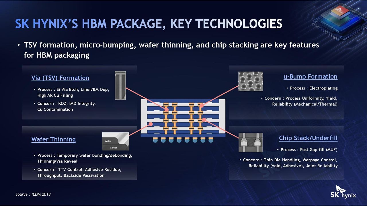
The race to power the next generation of artificial intelligence is currently being fought in the microscopic world of memory packaging. As memory capacity continues to explode, the challenge isn’t just making chips faster; it’s figuring out how to stack memory components in a way that maximizes density without sacrificing performance or cooling capabilities.
At the heart of this challenge is hybrid bonding, a revolutionary technique that aims to connect components using copper-to-copper bonds. However, ambitious goals for future memory solutions, like HBM4E and beyond, run straight into physical constraints. As SK hynix’s VP of package engineering, Jaesik Lee, explained at Hot Chips 2026, the industry’s most anticipated memory packaging transition is currently being pushed out to HBM5 as the earliest realistic target.
The primary hurdle is physical space. Standard logic wafers dictate a maximum package thickness of 775 microns. This ceiling creates a bottleneck: every additional layer of DRAM must be squeezed into thinner dies and narrower gaps, increasing manufacturing complexity.
This miniaturization introduces severe thermal problems. Thinner dies mean more oxide and poorer heat conduction compared to silicon. SK hynix estimates that the thermal burden across these memory generations is 2.2 times higher, forcing engineers to seek radical solutions for cooling.
To combat this heat, SK hynix introduced the iHBM cooling architecture. This concept embeds thermally conductive and electrically insulating blocks directly into the base die’s interface hotspot, targeting a potential reduction in thermal resistance of over 30%. While this solution offers massive thermal gains, Lee noted that because these blocks are integrated into the core design, they are a co-design effort and cannot be applied to memory generations already in design.
Despite the promise of bonding, fully realizing multi-layer stacks remains complex. Hybrid bonding for 20-layer and above stacks is still in the research phase. While initial orders for bonding techniques have been placed, the full-scale implementation of this process is projected to enter full-scale HBM production with HBM5 around 2029 to 2030.
Further complicating the picture is the trade-off between bandwidth and capacity. Some analysts argue that simply stacking memory height inherently slows down average memory access speeds compared to alternatives like DDR5. However, the solution may lie not in sheer height, but in intelligent memory placement—splitting workloads between high-bandwidth HBM and traditional LPDDR memory. This tiered approach, combined with innovations in high-bandwidth flash technology, offers a promising path forward for maximizing performance in the next wave of AI accelerators.
Credit
