Slipping product results in Absolics final qualification
The Glass Revolution: Why the Future of Chips is Going Beyond Silicon
A revolutionary shift is underway in the world of semiconductor packaging, where a material once relegated to novelty is now pushing the boundaries of what is physically possible. Glass-core substrates, poised to replace traditional organic chip packaging, offer a pathway to solving the immense physical and density challenges facing next-generation processors. This ambitious transition, backed by massive investment and fierce competition, is moving from theoretical promise to the crucial stage of final qualification.
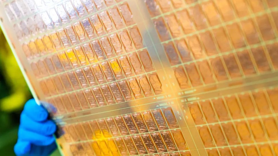
At the heart of this revolution is the physics. The technical appeal of glass lies in its ability to handle extreme density and thermal stress far better than conventional organic materials. Glass offers ten times the interconnect density, allowing for intricate wiring that traditional substrates simply cannot manage. Furthermore, glass cores boast a significantly lower thermal expansion coefficient, allowing them to minimize the warpage and distortion that plague silicon-based packages. This makes glass a material ideally suited for the complex, multi-chiplet architectures that define modern computing.
Beyond thermal advantages, glass opens up new architectural possibilities. Innovations like through-glass vias, demonstrated with impressive aspect ratios, allow for internal connectivity that drastically reduces signal latency. Researchers have also successfully demonstrated stacked glass running at high frequencies, paving the way for ultra-fast communication within integrated systems.
Despite the compelling technical case, manufacturing glass substrates is not without its hurdles. The transition demands extreme precision. Early attempts faced significant challenges with chip fracturing at the edges during the drilling and dicing processes. Overcoming these issues requires sophisticated edge-coating techniques and new low-temperature dielectrics to manage thermal stress during fabrication. Achieving the nanometer-scale flatness and perfect metallization required for mass production remains an open manufacturing problem.
The race to commercialization involves a coalition of global giants. Intel, having initiated the drive, is licensing patents and demonstrating working systems, aiming for deployment around 2030. Meanwhile, major industry players are structuring massive joint ventures. For instance, a substantial collaboration has been formalized between Samsung Electro-Mechanics and Sumitomo Chemical’s Dongwoo Fine-Chem, aiming for production capabilities by the second half of 2027.
The manufacturing backbone is being built across continents. In the United States, a $600 million facility in Georgia, backed by CHIPS Act funding, is scaling up substrate production, targeting mass output by late 2026. Simultaneously, efforts are intensifying in Asia, with Samsung pursuing a similar strategy, and Japan focusing on panel-level packaging and advanced glass techniques. Companies like TSMC are also exploring glass integration, aiming to position their massive packaging operations to leverage this new material.
The market potential is staggering. Analysts project the advanced IC substrate market to reach $31 billion by 2030, with glass cores expected to be a major growth driver. As the industry pushes toward next-generation processors—like Nvidia’s Rubin Ultra—which demand exponentially higher interconnect density, the demand for materials that can handle this density is skyrocketing. While specific commercial product timelines are still being finalized, the momentum behind glass-core technology suggests that the future of computing will indeed be built on the unique properties of glass.
Buy on Amazon
Credit
