TSMC 6 microns and the unexpected HBM delay in Hybrid Bonding
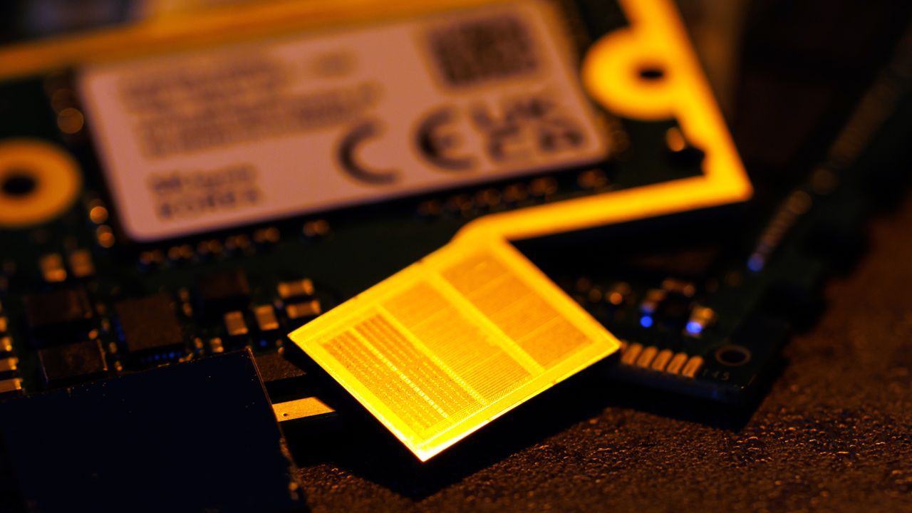
The future of semiconductor packaging is being redefined by a technique that promises to shatter the limitations of traditional chip stacking: hybrid bonding. This revolutionary method replaces the humble solder microbumps in 3D chip stacks with direct copper-to-copper connections, allowing components to be joined face-to-face with unprecedented density and speed.
At its core, hybrid bonding achieves this by polishing two dies flat and directly bonding their copper pads and surrounding dielectric layers under heat and pressure, eliminating the need for intermediary solder bumps. This fundamental shift allows connections to be packed far tighter, yielding an interconnect density roughly fifteen times greater than conventional 2.5D microbump stacking. For instance, early demonstrations suggest face-to-face bonding can achieve around 14,000 signals per square millimeter.
The scaling potential of this technology is staggering. While the method is already seeing high-volume production in logic chips, major players are pushing pitches down dramatically. TSMC, for example, has outlined a roadmap to shrink its System on Integrated Chip (SoIC) bond pitch from 9 microns today down to 6 microns and even targeting 4.5 microns by 2029. Similarly, Intel is deploying its Foveros Direct hybrid bonding in high-volume server CPUs, with plans to further refine the connection pitch toward 3 microns.
The mechanics of hybrid bonding involve two main approaches: wafer-to-wafer bonding, which offers the tightest pitch and fastest production, and die-to-wafer bonding. The latter is particularly crucial for modern chiplet architectures, enabling the mixing of different die sizes and process nodes, as required by high-bandwidth memory (HBM) and advanced accelerators.
While logic chip makers are rapidly adopting this method, the integration into high-bandwidth memory (HBM) has hit a temporary pause. A JEDEC decision to raise the HBM stack-height limit has deferred the arrival of hybrid bonding in memory, pushing its expected debut into HBM4E and HBM5 at the end of the decade.
Despite the delay in memory, the packaging infrastructure is booming. Memory manufacturers like SK hynix and Micron are investing billions into advanced-packaging facilities, preparing for the inevitable volume. Furthermore, competitors are not sitting still; Samsung is exploring similar solutions with its SAINT packaging family, and companies are scrambling to develop the specialized tools needed for this cutting-edge process.
The race for efficiency is now centered on tooling. Companies like Applied Materials and Besi are leading the development of integrated die-to-wafer bonding systems, demonstrating the industry’s commitment to making hybrid bonding a reality. Even as logic products evolve, the memory market is demanding these denser, faster interfaces, ensuring that hybrid bonding will remain a defining feature of the next generation of semiconductor technology.
Buy on Amazon
Credit
