TSMC Samsung Intel deploy larger High-NA EUV photomasks
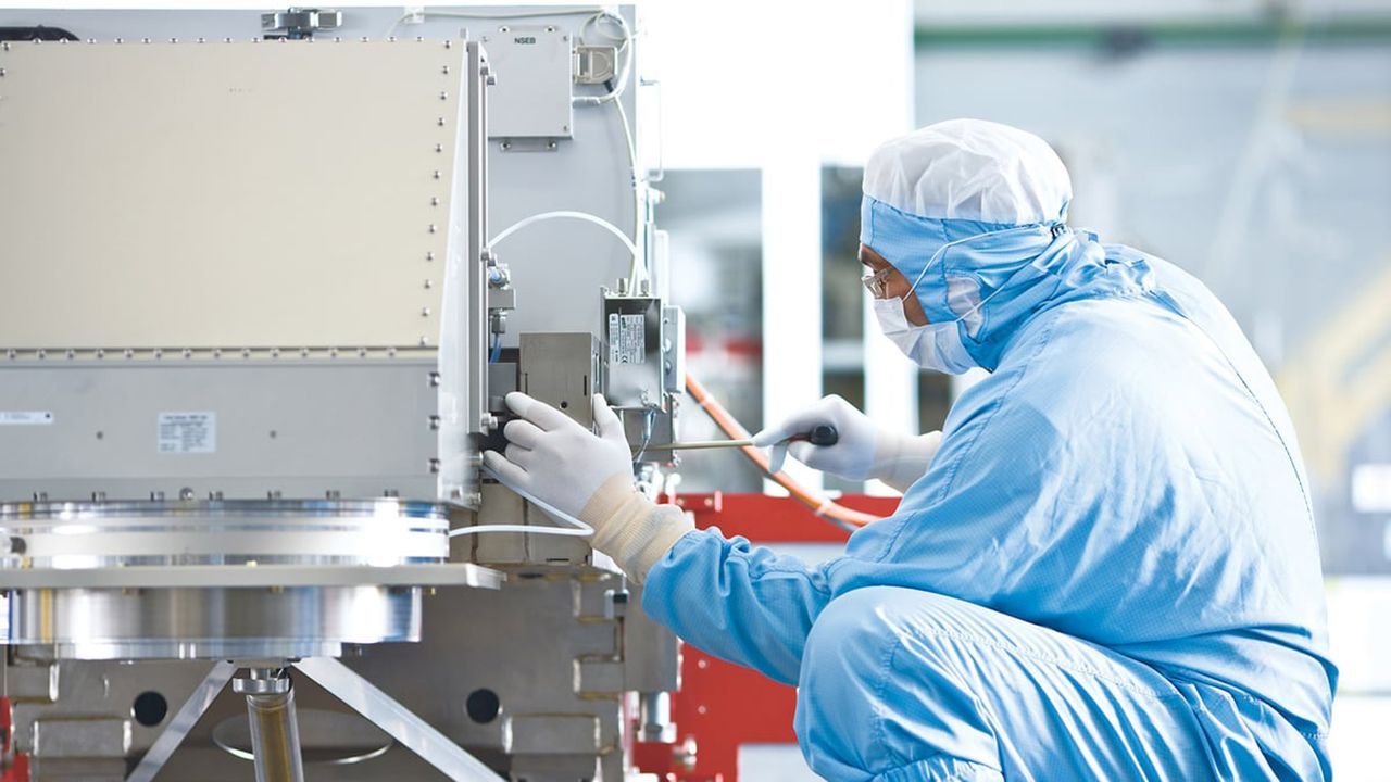
The world of semiconductor manufacturing is undergoing a dramatic transformation, driven by a powerful collaboration between giants like ASML, Intel, Samsung, and TSMC. To unlock the next level of performance in chip design, the industry is pivoting toward a monumental change in how they handle lithography: moving from traditional 6×6-inch photomasks to larger 6×12-inch reticles.
This isn’t just a change in dimensions; it’s a strategic move necessary for High-NA EUV lithography. High-NA systems offer significantly higher resolution, allowing chipmakers to pattern smaller, denser features in a single exposure. This potential gain promises to reduce the number of process steps, shorten manufacturing cycles, and ultimately boost the fidelity and yield of next-generation technologies.
However, achieving this higher resolution introduces a fascinating engineering challenge. Conventional Low-NA EUV systems relied on larger optics and standard masks to achieve a broad exposure field. High-NA EUV, with its anamorphic optics, operates differently. To make the shift seamless, chipmakers initially relied on stitching—piecing together multiple exposures—a workaround that works but comes with substantial costs.
Stitching, while workable in the short term, is not a perfect solution. It introduces performance bottlenecks. For instance, throughput drops significantly when stitching is used, and the critical requirement of aligning these exposures with extreme precision means that tiny errors can translate into defects, severely impacting the costly yield of advanced processors.
To eliminate the complexity and risk of stitching, the industry is exploring a radical solution: larger 6×12-inch photomasks. By doubling the reticle dimension, these larger masks are designed to compensate for the anamorphic optics, restoring the full exposure field and enabling the patterning of even larger dies in a single step.
This ambition requires a complete overhaul of the supply chain. Mask suppliers, like AGC and Hoya, must develop new equipment to produce larger substrates with uniform reflective multilayers. Mask shops will need redesigned writers and inspection systems, while mask handling infrastructure must be upgraded to accommodate larger pods and automated systems.
Perhaps the most profound change will come from ASML, whose High-NA EUV scanners will need redesigns to handle these substantially larger reticles with the required precision. This transition demands a coordinated effort, seeing as the industry must manage both the legacy 6×6-inch format and the new 6×12-inch format simultaneously.
While the 6×12-inch masks offer tremendous value for massive designs, such as high-end AI accelerators and data center CPUs that demand a full 26×33 mm exposure field, the existing 6×6-inch format remains vital for the vast majority of standard client processors. The industry is moving toward a phased adoption, with Intel leading the charge and setting ambitious timelines to achieve full lithography system readiness for advanced-node production by 2033.
Buy on Amazon
Credit