TSMC starts High-NA EUV in 2030 for A10/A11
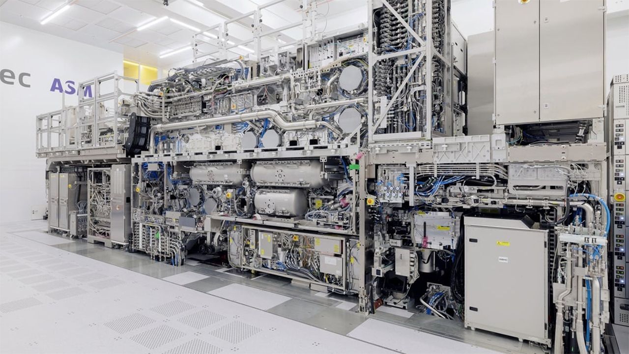
The future of semiconductor manufacturing is unfolding at warp speed, and the race to build smaller, faster, and more powerful chips is demanding increasingly sophisticated tools. At the heart of this technological evolution is the shift toward High-NA EUV lithography, a monumental change that TSMC is now actively planning to implement.
For years, the industry has grappled with the balance between technological advancement and cost. While developers sought ways to push boundaries in process technology without relying on multi-hundred-million-dollar scanners, TSMC maintained a cautious public stance regarding High-NA EUV systems, opting to keep strategy under wraps.
However, the limitations of current Low-NA EUV systems mean that the company cannot wait indefinitely. This week, TSMC unveiled its commitment: they plan to begin utilizing High-NA EUV lithography for high-volume manufacturing starting in 2030.
This transition involves an ambitious, phased approach. Initially, TSMC intends to use High-NA EUV with conventional 6×6-inch photomasks in 2030. This is followed by a strategic move toward larger mask formats, with plans to build a pilot line utilizing 6×12-inch photomasks in 2031.
The ultimate goal is to integrate 6×12-inch High-NA lithography systems into advanced node production by 2033. This shift is crucial because High-NA EUV can deliver an 8nm single-exposure resolution, offering significant improvements over the 13nm resolution provided by current Low-NA systems.
This evolution isn’t without technical hurdles. While High-NA EUV promises superior resolution, using conventional 6×6-inch masks results in half the exposure field compared to Low-NA counterparts. This presents challenges for manufacturing massive dies, such as complex AI accelerators, forcing chipmakers to consider solutions like multi-chiplet designs.
To overcome the 6×6-inch mask limitation and unlock the full potential of this technology, TSMC is actively collaborating with ASML to set the stage for the transition to 6×12-inch photomasks. This change requires a sweeping overhaul of the entire ecosystem, impacting everything from Electronic Design Automation (EDA) software to the tools that produce and handle the masks.
ASML, the supplier of these critical tools, appears highly optimistic about this transition, noting that the move is supported by major semiconductor manufacturers. Christophe Fouquet, President & CEO of ASML, stated that the adoption of High-NA EUV will increase along the device scaling roadmap, enabling greater scanner productivity and supporting the demand for smaller, faster, and more energy-efficient chips.
The biggest question remaining is which process technology will pioneer this adoption. Based on existing roadmaps, candidates like A10 or A11 (1/1.1nm-class) are strong contenders for leveraging High-NA EUV for the most critical layers. As TSMC continues its strategy, the evolution of node technologies, potentially leveraging TSMC’s 3rd Generation nanosheet GAA transistors, will dictate the speed and scope of this exciting technological leap.
Buy on Amazon
Credit