Zeiss expansion caps ASML EUV output
At the razor edge of semiconductor manufacturing, where technology moves faster than light, the physical reality of optical engineering dictates the pace of progress. This is the story of how specialized precision—driven by Carl Zeiss SMT—is powering the world’s most advanced lithography systems.
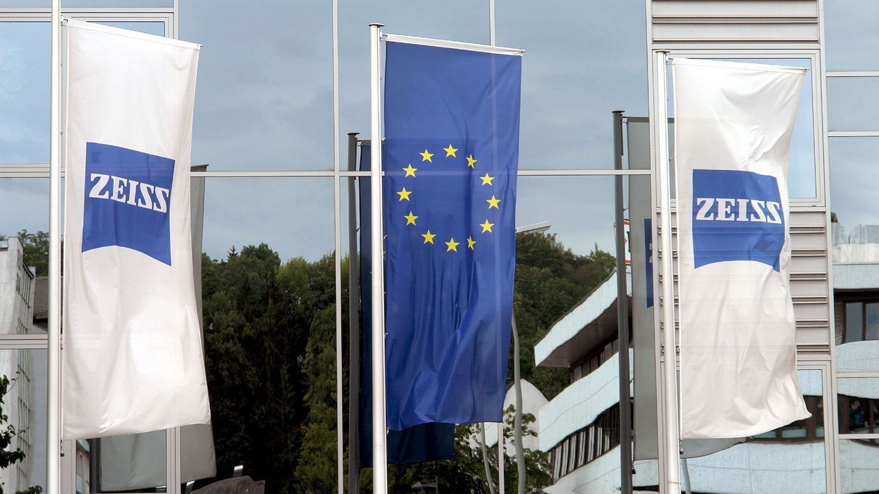
The engine room for cutting-edge chip production resides in southern Germany, where Carl Zeiss Semiconductor Manufacturing Technology is significantly boosting its capacity. The company is expanding its production and adjacent space at Oberkochen, adding around 25,000 square meters of facilities. This expansion means that staff are now moving into the first completed building this month, marking a major step forward four years after the initial groundbreaking in 2022. While more construction remains, this move signals an intense commitment to scaling up the capabilities required by industry leaders.
This operational capacity is not just an internal matter; it touches the global supply chain for quantum-level technology. Oberkochen and Wetzlar stand out as unique locations globally where the critical optical columns within ASML’s lithography scanners must be built. In essence, the output of ASML itself is fundamentally limited by Zeiss SMT’s production capability.
The stakes for these components are monumental. As semiconductor technology pushes toward extreme resolution, the demands on optics escalate dramatically. The creation of High-NA projection optics involves an astonishing complexity: more than 40,000 parts and weighing about 12 tons. Furthermore, the specialized mirrors required for this work are massive; individual High-NA mirrors can be twice the size and ten times the weight of current EUV mirrors, requiring months of meticulous machining before they reach specification.
Verifying these complex optics demands even more specialized infrastructure, including a purpose-built vacuum chamber measuring 5 by 10 meters, packed with over 100,000 parts and weighing more than 150 tons. This level of engineering ensures that every lens and mirror functions flawlessly, enabling processes like the transition to Low-NA EUV, which ASML plans to boost by roughly 30% in 2027.
The critical dependency is underscored by the financial relationship between the two giants. In 2025, purchases from Zeiss SMT and its subsidiaries reached €4.41 billion, demonstrating the immense economic leverage of this exclusive arrangement. If Zeiss SMT were to face production constraints over a prolonged period, the warning issued indicates that ASML would effectively be unable to conduct its core business.
This symbiotic relationship is driving innovation across the board. ASML itself is working to compress its scanner build cycle from approximately 22 weeks down to just 15 or 16 weeks, a move that aligns with the high-speed demands of modern chip fabrication. The financial flows reflect this commitment, with ASML holding €1.91 billion in loans receivable from Zeiss SMT at year-end 2025, underscoring the tangible value of these bespoke optical components.
Beyond immediate production, Carl Zeiss SMT continues to expand its global footprint, building new multifunction factories in Wetzlar and adding substantial cleanroom space. This growth is further supported by strategic investments, including an innovation center in Korea, solidifying the company’s role not just as a supplier, but as a central force in the future of high-precision semiconductor technology.
Credit