
Visualize Musk’s Terafab massive footprint vs. famous landmarks
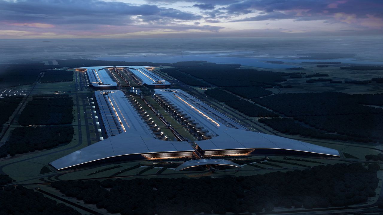
When you talk about building the future of technology, you often think in terms of incremental steps and careful planning. But when the conversation shifts to megafactories, things get wonderfully, impossibly ambitious. Elon Musk’s Terafab project is one such endeavor—a colossal vision that is rapidly moving from theoretical blueprint to concrete reality, demonstrating how quickly audacious ideas can translate into massive physical infrastructure.
Less than five months after the initial announcement, a recent drone flyover of the Texas site revealed something truly staggering: progress has already begun on the ground. This isn’t just another factory; it is designed to be an unprecedented ecosystem for semiconductor manufacturing, dwarfing existing industrial complexes in sheer scale.
To grasp the magnitude, imagine the potential footprint. Reports suggest the facility will require at least 100 million square feet of floor space. To put that into perspective, this single site would encompass more total space than several major landmarks combined, including Giga Texas, the Pentagon, Apple Park, and the Mall of America, taken together.
This immense size isn’t arbitrary; it reflects the complexity of the vision. The Terafab is not just intended to produce AI processors, but to be an all-in-one manufacturing hub. It aims to integrate every critical step—from designing and fabricating logic and memory chips to handling lithography, packaging, and testing—all under one roof.
The impetus for such a gargantuan effort lies in the skyrocketing demand for advanced semiconductors fueled by artificial intelligence. As Nvidia CEO Jensen Huang warns, meeting this monumental computational need is an “extremely hard” challenge for the industry. This pressing shortage has spurred giants like Tesla and SpaceX to seek radical solutions, leading Musk to pursue his own chip manufacturing facility as a necessary answer.
This pursuit of unconventional methods is attracting powerful industry figures. Intel CEO Lip-Bu Tan has publicly acknowledged that he sees no better partner than Elon Musk to explore the “unconventional ways” needed to revolutionize how chips are made and drastically reduce costs.
Musk’s history is marked by an extraordinary willingness to tackle seemingly impossible engineering feats. From revolutionizing commercial space travel with SpaceX to setting records for processing massive amounts of GPU hardware in record time, his trajectory suggests a relentless drive toward solving the seemingly intractable. The Terafab project represents perhaps his largest undertaking yet, estimated to require up to $119 billion in investment.
While the potential reward is staggering, the journey ahead is fraught with complexity. Despite the strong customer base provided by SpaceX and Tesla, there remains an inherent risk that this ambitious megafactory may not reach its full potential. It is a high-stakes gamble—a testament to the idea that true innovation often requires embracing risks on a scale never before attempted.
Credit