
China’s chipmaking roadmap: DUV and EUV tool goals
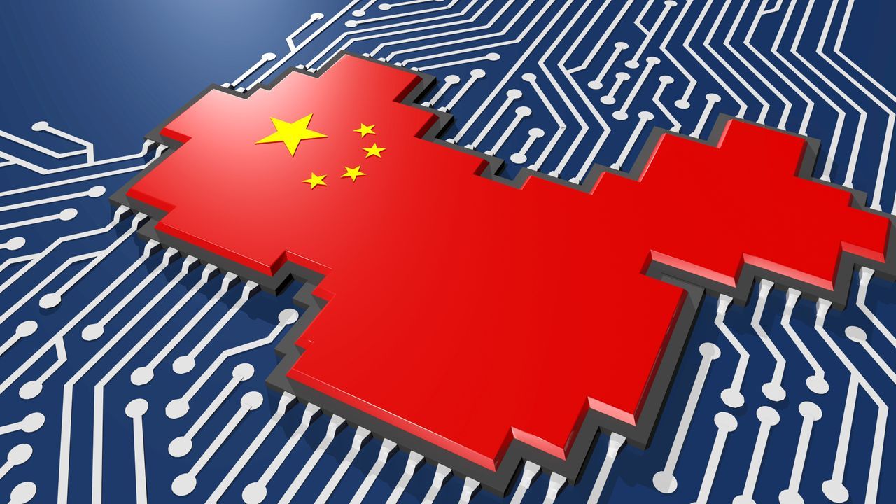
The world of semiconductor manufacturing is currently being defined by a monumental race for self-sufficiency, pitting global technology giants against ambitious national programs. At the heart of this technological contest is the drive to localize the most critical tools for chip production, specifically the advanced lithography systems that define modern microprocessors.
China has launched an aggressive strategy to develop its own domestic immersion DUV lithography machines, aiming to reshape the global supply chain and significantly diminish reliance on foreign technology. This endeavor has already sent ripples through the market, reportedly wiping nearly 44 billion dollars off ASML’s market value.
To power this initiative, a new state-owned entity named Shanghai Aishengna Electronic Technology Group was established in August 2023. This group successfully absorbed engineering talent from various affiliated startups and state scanner makers, pooling resources to create an ambitious roadmap for domestic tool manufacturing. The plan calls for five such systems this year, with the target climbing to roughly twenty by 2027.
While these goals are staggering, the technical reality involves navigating complex dependencies. Immersion lithography is a highly specialized field, and even the pioneering Chinese tools are still in the validation phase. They currently operate far behind the capabilities of established leaders like ASML‘s flagship models, which set the benchmark for performance metrics such as throughput and overlay accuracy.
The global immersion market remains overwhelmingly dominated by Europe; ASML commands an estimated 98.7% of the total systems deployed annually. China’s current contribution to this landscape is small, representing only about 3.8% of the total immersion systems currently in use.
Significant progress has been made at the foundry level. China’s largest semiconductor manufacturer has pursued its own domestic immersion scanner, developed under the codename Mount Everest. This effort, alongside other domestic developments involving companies like Yuliangsheng and SMEE, reflects a concerted push toward internal capabilities.
Despite these developments, the path to full localization faces structural challenges. Many essential components required for these advanced machines are still imported from Japan. Delays in securing these components have capped production targets, meaning that achieving the 20-system goal by 2027 requires a level of domestic component maturity that has yet to be fully established.
Furthermore, the broader semiconductor equipment sector remains highly fragmented. Industry leaders have acknowledged that the domestic tool landscape is currently small, fragmented, and weak, prompting calls for national consolidation and redirection of significant funds toward lithography and EDA development. This pressure drives the necessity for these state-backed ventures to succeed.
The geopolitical backdrop further heightens the stakes. New export control measures aim to restrict access to critical technologies, impacting the installed base of advanced equipment globally. Consequently, Chinese fabs are actively exploring ways to utilize older tools and third-party components while pushing forward with domestic development. The ultimate validation of China’s DUV program will come down to tangible results: validated production wafers, demonstrated throughput figures, and achieved yield rates from these new domestic systems.
Buy on Amazon
Credit